Chip packaging manufacturing equipment

A technology for manufacturing equipment and chip packaging, which is applied in semiconductor/solid-state device manufacturing, transportation and packaging, electrical components, etc. It can solve the problems of high labor cost, inability to realize automatic continuous production, and low production efficiency, so as to avoid follow-up testing, Improve the effect of continuous production

Pending Publication Date: 2022-06-28
深圳市星芯科技有限公司
View PDF0 Cites 0 Cited by
  • Summary
  • Abstract
  • Description
  • Claims
  • Application Information

AI Technical Summary

Problems solved by technology

[0003] In the prior art, when the chip is packaged, it is necessary to manually load and unload the material. During the operation, the shell and the chip body are manually put into the welding equipment, and the chip body and the body on the shell are welded by the welding equipment. The pins are soldered and packaged with an adhesive. After the package is completed, the packaged chip needs to be tested to determine whether it is normal. In the above steps, manual participation is required, which requires a lot of labor and high labor costs. And when manually connecting the chip body and the shell, it is easy to shift, resulting in damage to the chip and making it unusable, and automatic continuous production cannot be realized, and the production efficiency is low

Method used


Image

  • Chip packaging manufacturing equipment
  • Chip packaging manufacturing equipment
  • Chip packaging manufacturing equipment

Examples


Embodiment 1

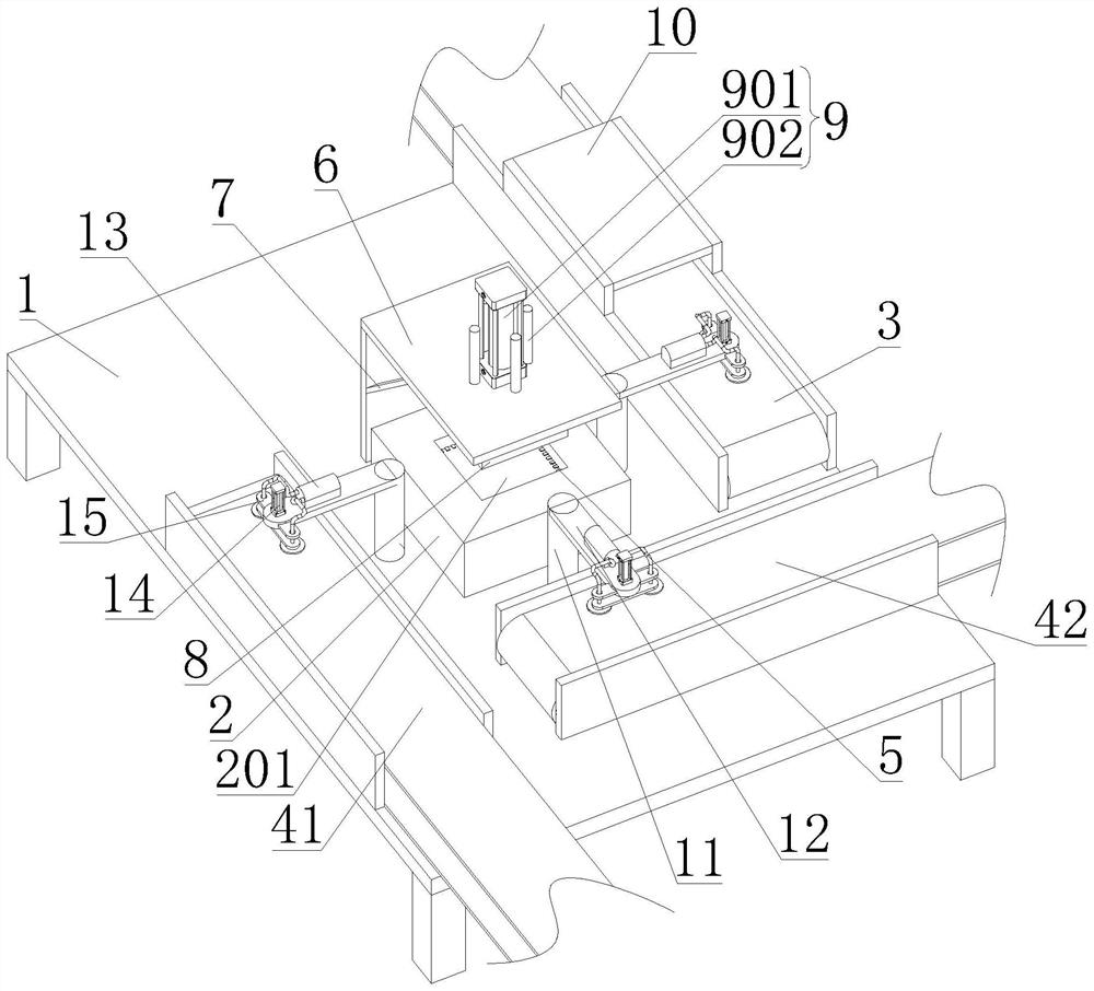
[0030] like Figure 1-3 As shown in the figure, a chip packaging manufacturing equipment proposed by the present invention includes a workbench 1, a packaging table 2, a feeding mechanism 3, a feeding mechanism 41, a feeding mechanism 42, a detection contact 5, a support frame 6, a welding Mechanism 8, rotating column 11, support arm 12 and adsorption mechanism 13;

[0031] The packaging table 2, the unloading mechanism 3, the a feeding mechanism 41, the b feeding mechanism 42 and the support frame 6 are all arranged on the work table 1; the packaging table 2 is provided with a positioning groove 201; the detection contact 5 is arranged in the positioning groove 201; the welding mechanism 8 is slidably arranged above the positioning groove 201; the supporting frame 6 is provided with a lifting mechanism 9 for driving the welding mechanism 8 to move; three rotating columns 11, support arms 12 and adsorption mechanisms 13 are provided; One end of 12 is arranged on the upper end...

Embodiment 2

[0045] like Figure 1-3 As shown in the figure, a chip packaging manufacturing equipment proposed by the present invention, compared with the first embodiment, the lifting mechanism 9 in this embodiment includes a telescopic cylinder 901 and a guide rail 902; a telescopic cylinder 901 is arranged on the support frame 6, a telescopic The output end of the cylinder 901 is connected with the upper end of the welding mechanism 8 .

[0046] In this embodiment, after the casing and the chip body are placed in the positioning groove 201, a telescopic cylinder 901 drives the welding mechanism 8 to move downward, and the guide rail 902 guides and supports the welding mechanism 8, so that the welding mechanism 8 moves more easily Stable, the welding mechanism 8 is in contact with the chip body, so that the chip body and the pins can be welded together, and packaging can be performed.

Embodiment 3

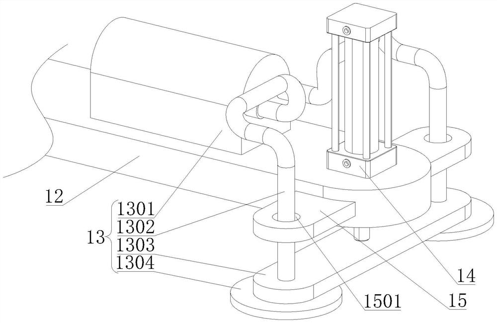
[0048] like Figure 1-3 As shown, in a chip packaging manufacturing apparatus proposed by the present invention, compared with Embodiment 1 or Embodiment 2, the adsorption mechanism 13 in this embodiment includes an air pump 1301, a communication pipe 1302, a lifting plate 1303 and a suction cup 1304; the air pump 1301 is provided with On the support arm 12; a plurality of communicating pipes 1302 and suction cups 1304 are provided; a plurality of suction cups 1304 are arranged on the lower end of the lift plate 1303; the lift plate 1303 is slidably arranged on the lower end of the support arm 12; The lift plate 1303 is driven to move the telescopic cylinder 14; the two ends of the communication pipe 1302 are respectively connected with the air pump 1301 and the suction cup 1304. The support arm 12 is provided with a support plate 15 , and the support plate 15 is provided with a guide groove 1501 ;

[0049] In this embodiment, taking the casing on the feeding mechanism 41 for...


PUM


Abstract

The invention relates to chip packaging manufacturing equipment, which belongs to the technical field of chip packaging and comprises a workbench, a packaging table, a discharging mechanism, a feeding mechanism a, a feeding mechanism b, a detection contact, a supporting frame, a welding mechanism, a rotating column, a supporting arm and an adsorption mechanism. A positioning groove is formed in the packaging table; the detection contact is arranged in the positioning groove; the welding mechanism is arranged above the positioning groove in a sliding manner; a lifting mechanism used for driving the welding mechanism to move is arranged on the supporting frame. The rotating column is rotationally arranged on the workbench; a driving mechanism for driving the rotating column to rotate is arranged on the workbench; limiting mechanisms are arranged at the lower ends of the rotating columns; the discharging mechanism, the feeding mechanism a, the feeding mechanism b, the welding mechanism, the lifting mechanism, the adsorption mechanisms, the limiting mechanism and the driving mechanism are all in communication connection, and the three adsorption mechanisms are located above the discharging mechanism, the feeding mechanism a and the feeding mechanism b correspondingly. According to the invention, the chip can be automatically loaded and packaged, and the packaged chip can be taken down.

Description

technical field [0001] The invention relates to the technical field of chip packaging, in particular to a chip packaging manufacturing equipment. Background technique [0002] The casing used for installing the semiconductor integrated circuit chip plays the role of placing, fixing, sealing, protecting the chip and enhancing the electrical and thermal performance, and it is also a bridge to communicate the internal world of the chip and the external circuit - the contacts on the chip are connected to the package casing with wires. On the pins, these pins are connected with other devices through wires on the printed board. After the chip body and the pins on the casing are welded, the chip body and the casing are connected by adhesive to complete the package. [0003] In the prior art, when the chip is packaged, it needs to be manually loaded and unloaded. During the operation, the shell and the chip body are manually put into the welding equipment, and the chip body and the ...

Claims


Application Information

Patent Timeline
Patent Type & Authority Applications(China)
IPC IPC(8): H01L21/67H01L21/677
CPCH01L21/67121H01L21/67276H01L21/67742H01L21/6776
Inventor 张莉李双喜
Owner 深圳市星芯科技有限公司
Why Eureka
Try Eureka