Multi-chip three-dimensional stacked structure with electromagnetic shielding function and preparation method thereof

An electromagnetic shielding, three-dimensional stacking technology, applied in circuits, electrical components, electrical solid devices, etc., can solve problems such as crosstalk and electromagnetic interference, and achieve the effect of increasing the heat dissipation effect

Pending Publication Date: 2022-06-28
JCET SEMICON (SHAOXING) CO LTD
View PDF0 Cites 0 Cited by
  • Summary
  • Abstract
  • Description
  • Claims
  • Application Information

AI Technical Summary

Problems solved by technology

[0006] Aiming at the deficiencies in the prior art, the present invention provides a multi-chip three-dimensional stacking structure with electromagnetic shielding function that can solve the problems of electromagnetic interference and signal crosstalk in the prior art and improve thermal conductivity. its preparation method

Method used


Image

  • Multi-chip three-dimensional stacked structure with electromagnetic shielding function and preparation method thereof
  • Multi-chip three-dimensional stacked structure with electromagnetic shielding function and preparation method thereof
  • Multi-chip three-dimensional stacked structure with electromagnetic shielding function and preparation method thereof

Examples


Embodiment Construction

[0051] The technical solutions in the embodiments of the present invention will be clearly and completely described below with reference to the accompanying drawings in the embodiments of the present invention. Obviously, the described embodiments are only a part of the embodiments of the present invention, but not all of the embodiments. Based on the embodiments of the present invention, all other embodiments obtained by those of ordinary skill in the art without creative efforts shall fall within the protection scope of the present invention.

[0052] In order to make the objectives, technical solutions and advantages of the present invention clearer, the present invention will be further described in detail below with reference to the accompanying drawings and embodiments. It should be understood that the specific embodiments described herein are only used to explain the present invention, but not to limit the present invention.

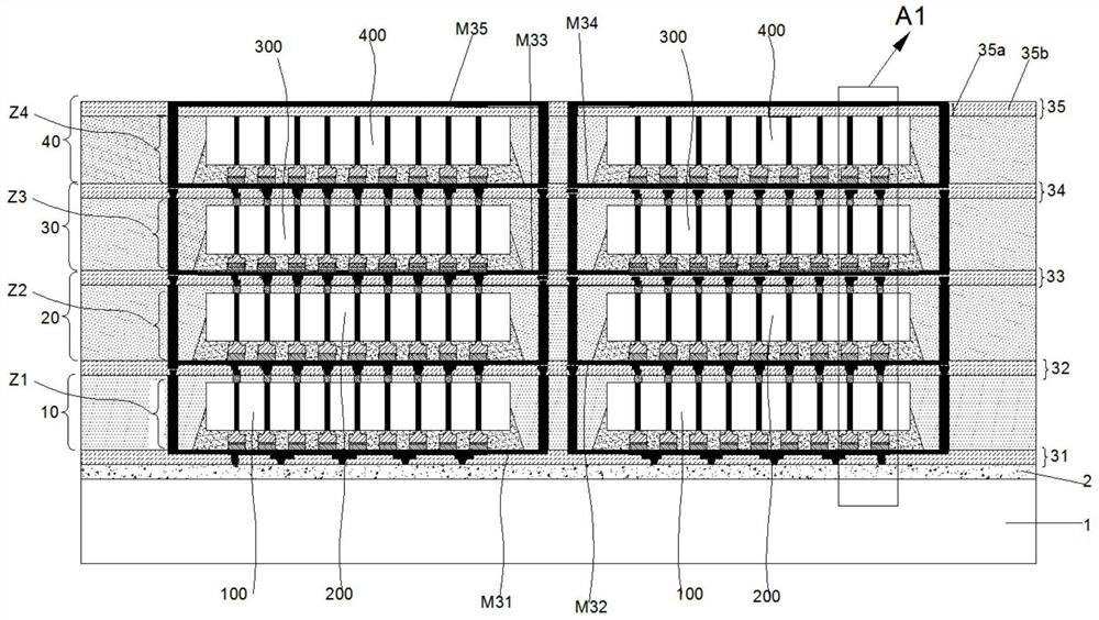
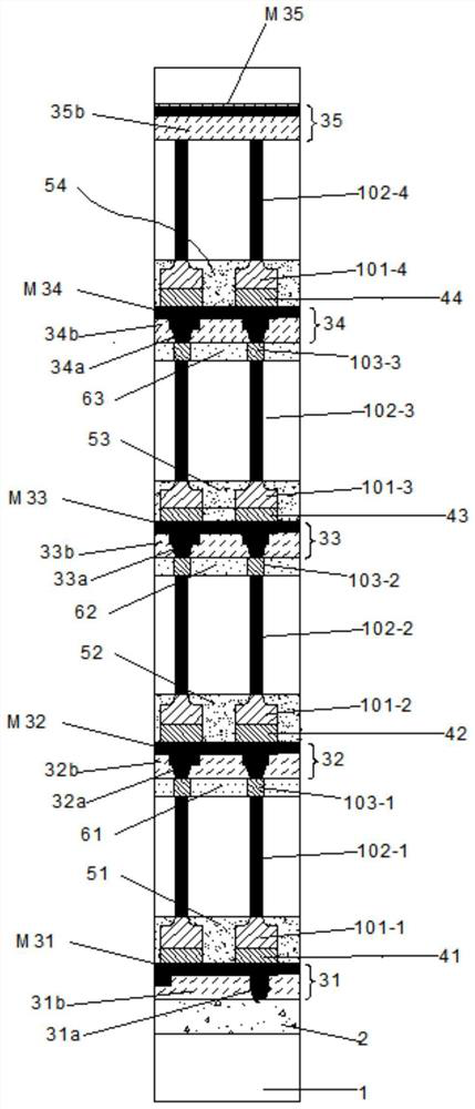
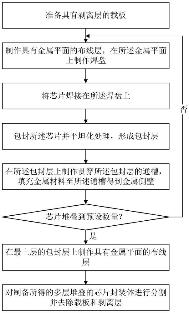
[0053] In a first aspect, a multi-chip thre...


PUM


Abstract

The invention discloses a multi-chip three-dimensional stacking structure with an electromagnetic shielding function, which comprises N wiring layers and N-1 encapsulation layers which are alternately stacked, a metal plane is arranged in each wiring layer, a chip and a metal side wall surrounding the chip are arranged in each encapsulation layer, and the metal side wall is arranged on the metal plane. And the metal side wall in each encapsulation layer is in closed connection with the metal planes in the two adjacent wiring layers so as to seal the chip in the encapsulation layer. The invention further discloses a preparation method of the multi-chip three-dimensional stacking structure with the electromagnetic shielding function. According to the invention, the electromagnetic interference problem and the signal crosstalk problem of the chip in the three-dimensional stacked structure are solved, and the heat dissipation effect of the three-dimensional stacked structure is also improved.

Description

technical field [0001] The invention belongs to the technical field of semiconductor packaging, and in particular relates to a multi-chip three-dimensional stacking structure with electromagnetic shielding function and a preparation method thereof. Background technique [0002] The three-dimensional stacked chip packaging structure can realize the integration of multiple chips in a small package space, and use the vertical interconnection structure between the chips in the longitudinal direction to shorten the channel for electrical signal connection between the chips. Therefore, this packaging structure has many advantages. These advantages, such as: lower signal transmission loss, lower power consumption, lower signal delay, smaller package size, and can also achieve wafer-level 3D packaging and 3D heterogeneous integration, which is the future high-end chip packaging technology development direction of the field. [0003] However, there are still two main problems to be ...

Claims


Application Information

Patent Timeline
Patent Type & Authority Applications(China)
IPC IPC(8): H01L23/552H01L23/367H01L25/065H01L23/31H01L21/50H01L21/56
CPCH01L23/552H01L23/367H01L25/0657H01L23/3107H01L21/50H01L21/56
Inventor 李宗怿丁晓春刘籽余倪洽凯柳坤何佳奕曾丹王嘉炜
Owner JCET SEMICON (SHAOXING) CO LTD
Why Eureka
Try Eureka