Semiconductor device

A semiconductor and device technology, applied in the field of semiconductor devices, can solve the problems of reducing mutual inductance, enhancing the electrical isolation of bonding wires, and deteriorating the electrical isolation performance of chip packaging structures, so as to reduce mutual inductance, solve electromagnetic interference problems, and improve electrical isolation degree of effect

Inactive Publication Date: 2013-11-27
TIANJIN UNIV
View PDF3 Cites 6 Cited by
  • Summary
  • Abstract
  • Description
  • Claims
  • Application Information

AI Technical Summary

Problems solved by technology

Electromagnetic interference between these bonding wires and between the bonding wires and other sensitive components forms a signal leakage path inside the chip, allowing power to be coupled to other ports through the leakage path, thereby deteriorating the electrical isolation in the chip package structure performance
[0007] In the related art, how to enhance the electrical isolation between the bonding wires and between the bonding wires and other sensitive components and reduce the mutual inductance in a small-size environment has not yet proposed an effective solution.

Method used


Image

  • Semiconductor device
  • Semiconductor device
  • Semiconductor device

Examples


Embodiment Construction

[0032] The following will clearly and completely describe the technical solutions in the embodiments of the present invention with reference to the accompanying drawings in the embodiments of the present invention. Obviously, the described embodiments are only some, not all, embodiments of the present invention. All other embodiments obtained by persons of ordinary skill in the art based on the embodiments of the present invention belong to the protection scope of the present invention.

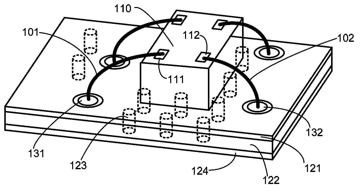
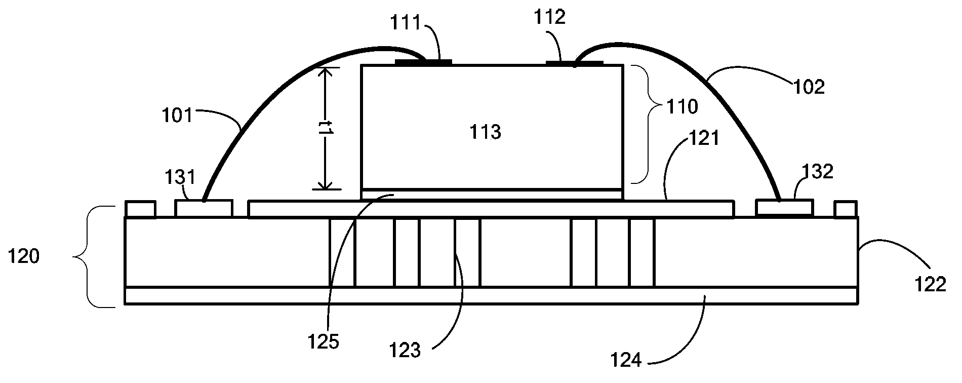
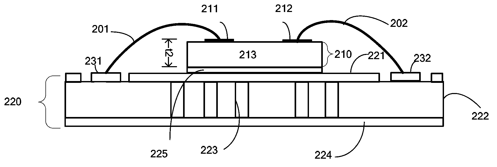
[0033] In the process of realizing the present invention, the inventor found that the electromagnetic interference in the radio frequency band chip is mainly produced by the mutual electromagnetic field interference between the bonding wires or between the bonding wires and other sensitive components, and the bonding wires are mutually And the electromagnetic interference between the bonding wire and other sensitive components has a very close relationship with the height of the bonding wire f...


PUM


Abstract

The invention discloses a semiconductor device. The semiconductor device comprises a package substrate including a bonding area used for connecting bonding wires; and at least one die provided on the package substrate. Each die comprises a wafer substrate and a pin disposed on the wafer substrate. Each pin is used for connecting the bonding wire. The thickness of each wafer substrate is between 50um to 400um. By thinning the wafer and reducing the thicknesses of the dies, the semiconductor device can reduce the average height of the bonding wires from a ground plane, thereby improving the electrical isolation between the bonding wires and between the bonding wires and other sensitive components, lowering mutual inductance, solving the problem of electromagnetic interference and improving chip performance.

Description

technical field [0001] The present invention relates to the field of semiconductor devices, in particular to a semiconductor device. Background technique [0002] In the semiconductor industry, a chip usually includes a die, a package carrier carrying the die, and other components. Package substrates include but are not limited to various forms such as stacked package substrates, LTCC substrates, and frame substrates. The electrical connection between the chip die and the package carrier is mainly achieved by bonding wires. Bonding wires are widely used in the semiconductor industry due to their advantages in productivity, reliability, and low cost. Bonding wires are usually made of metal materials, including but not limited to gold, copper, aluminum and other materials. According to the specific application requirements for the maximum power that the bonding wire can withstand, the diameter of the metal bonding wire varies from 15um to several hundred um. When the diame...

Claims


Application Information

Patent Timeline
Patent Type & Authority Applications(China)
IPC IPC(8): H01L29/06
CPCH01L24/73H01L2224/05554H01L2224/32145H01L2224/32225H01L2224/48091H01L2224/48145H01L2224/48227H01L2224/48235H01L2224/73265H01L2924/19042H01L2924/19105H01L2924/30107H01L2924/3025
Inventor 庞慰杨清瑞郑云卓张浩张代化
Owner TIANJIN UNIV
Why Eureka
Try Eureka