Image sensor and method for forming pixel structure of image sensor

An image sensor and pixel structure technology, applied in semiconductor devices, radiation control devices, etc., can solve the problem of image sensor white pixels, achieve the effect of improving white pixels and reducing metal ion pollution

Pending Publication Date: 2022-07-05
SHANGHAI HUALI MICROELECTRONICS CORP
View PDF0 Cites 1 Cited by
  • Summary
  • Abstract
  • Description
  • Claims
  • Application Information

AI Technical Summary

Problems solved by technology

[0004] The purpose of the present invention is to provide an image sensor and a method for forming the pixel structure of the image sensor, so as to propose a new method for forming vertical gate oxides, and to improve the problem of white pixels produced by the image sensor

Method used


Image

  • Image sensor and method for forming pixel structure of image sensor
  • Image sensor and method for forming pixel structure of image sensor
  • Image sensor and method for forming pixel structure of image sensor

Examples


Embodiment Construction

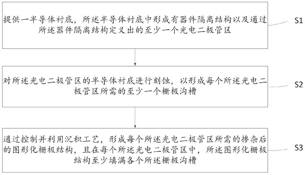
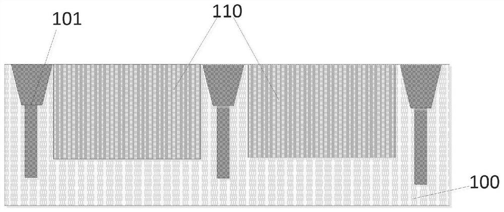
[0029] As described in the background art, at present, with the continuous advancement of the standard CMOS process level and the market demand for small-sized pixels, the pixel size of the CMOS image sensor has been gradually reduced from 5.6 mm to 1.0 mm. Nowadays, in order to increase the area of ​​the photodiode region PD, the pixel size has to be reduced. Therefore, the vertical gate oxide process emerges as the times require. Specifically, the existing method for forming vertical gate oxide is as follows: using silane to grow polysilicon in a low-voltage furnace tube, and then performing P ion implantation on the surface of the polysilicon layer formed as the gate structure to improve the K value of the polysilicon layer, In turn, the equivalent gate oxide thickness is reduced; however, the existing formation method will cause metal contamination in the CMOS image sensor product under the condition of small size, which will eventually cause the problem of white pixels.

...


PUM


Abstract

The invention provides an image sensor and a forming method of an image sensor pixel structure, and is applied to the technical field of semiconductors. In the forming method of the pixel structure of the image sensor provided by the invention, doping ions with controllable concentration and an adsorption effect are introduced in the process of growing a polycrystalline silicon gate structure in a low-pressure furnace tube by using silane in a traditional 55nm image sensor; the white pixel of the small-size image sensor is improved on the basis of reducing the metal ion pollution condition of the formed gate structure of the small-size image sensor.

Description

technical field [0001] The present invention relates to the technical field of semiconductors, and in particular, to an image sensor and a method for forming a pixel structure of the image sensor. Background technique [0002] CMOS image sensors have developed rapidly in the past ten years and are now widely used in mobile phones, computers, digital cameras and other fields. Generally, an active pixel unit of a CMOS image sensor includes a photodiode (PD) in an epitaxial layer and several transistors. Taking a 4T structure CMOS image sensor as an example, the four transistors specifically include a transfer tube 110 (Transfer, Tx). , source follower tube (Source Follow, SF), reset tube (Reset, RST) and row selection tube (Row Select, RS). Among them, the basic working principle of the CMOS image sensor is as follows: before lighting, turn on the reset tube and transfer tube to release the original electrons in the photodiode area; when lighting, turn off all transistors to ...

Claims


Application Information

Patent Timeline
Patent Type & Authority Applications(China)
IPC IPC(8): H01L27/146H01L21/28
CPCH01L27/14689H01L27/14614H01L21/28035
Inventor 刘琦王明李晓玉
Owner SHANGHAI HUALI MICROELECTRONICS CORP
Why Eureka
Try Eureka