Tiny defect detection method of printed circuit board and storage medium

A printed circuit board and defect detection technology, applied in the field of defect detection, can solve problems such as low stability and poor adaptability

Pending Publication Date: 2022-07-12
合肥综合性国家科学中心人工智能研究院
View PDF0 Cites 2 Cited by
  • Summary
  • Abstract
  • Description
  • Claims
  • Application Information

AI Technical Summary

Problems solved by technology

[0005] A micro defect detection method and storage medium of a printed circuit board proposed by the present invention can solve the technical problems of poor adaptability and low stability of existing methods in PCB defect detection

Method used


Image

  • Tiny defect detection method of printed circuit board and storage medium
  • Tiny defect detection method of printed circuit board and storage medium
  • Tiny defect detection method of printed circuit board and storage medium

Examples


Embodiment Construction

[0044]In order to make the purposes, technical solutions and advantages of the embodiments of the present invention clearer, the technical solutions in the embodiments of the present invention will be clearly and completely described below with reference to the accompanying drawings in the embodiments of the present invention. Obviously, the described embodiments These are some embodiments of the present invention, but not all embodiments.

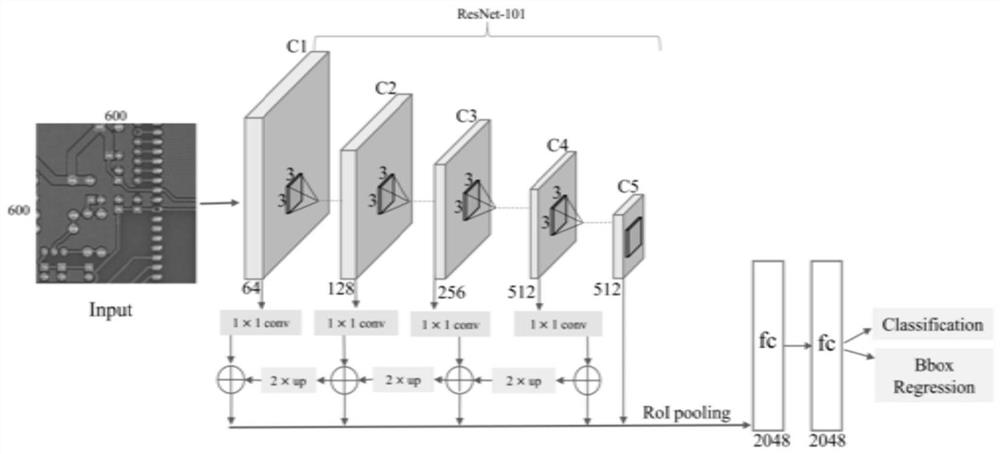
[0045] like figure 1 As shown, the method for detecting tiny defects of a printed circuit board described in this embodiment includes the following steps:

[0046] Step 1: Obtain PCB defect sample data and perform data preprocessing.

[0047] Step 2: Use k-means clustering on the bounding boxes of the PCB training set to find reasonable anchor scales.

[0048] Step 3: Extract features using a multi-scale feature pyramid structure. Upsampling the bottom-up feature map obtained in the backbone convolutional network to obtain a top-down fe...


PUM


Abstract

The invention discloses a micro defect detection method for a printed circuit board and a storage medium, and the method comprises the following steps: S1, obtaining PCB defect sample data, and carrying out the data preprocessing; s2, k-means clustering is used on a bounding box of the PCB training set to find an anchor scale meeting the requirement; s3, extracting features by adopting a multi-scale feature pyramid structure, performing up-sampling on a bottom-up feature map obtained in the trunk convolutional network to obtain a top-down feature map, and adding the top-down feature map and the bottom-up feature map element by element to obtain a final feature map; and S4, training network parameters by calculating loss. According to the method, sufficient training data required by deep learning is provided through a data enhancement technology, a reasonable anchor point scale is designed by using k-means clustering, and then a feature pyramid is combined with a Faster R-CNN network, so that the relationship between different levels of feature maps is enhanced, and the detection of the PCB tiny defects is realized. The method improves the detection efficiency, can adapt to detection of various defects, and is high in adaptability.

Description

technical field [0001] The invention relates to the technical field of defect detection, in particular to a method for detecting tiny defects of a printed circuit board and a storage medium. Background technique [0002] PCB is the carrier for the electrical interconnection of electronic components. In recent years, with the development of science and technology, PCB has been widely used in various electronic products, and the market size is huge. However, in the process of PCB manufacturing, visual defects of product quality are checked for PCB. The production adds huge costs. [0003] Considering that different PCBs in the real market have different complex wiring design rules, the existing general algorithms are difficult to be compatible with various PCBs, and the types and characteristics of PCB defects are generally diverse, so traditional PCB defect detection methods may have inconsistencies. Stability, low adaptability issues. [0004] Since 2014, deep learning met...

Claims


Application Information

Patent Timeline
Patent Type & Authority Applications(China)
IPC IPC(8): G06V10/774G06V10/762G06V10/40G06V10/20G06K9/62G06T7/00G06N3/04
CPCG06T7/0004G06T2207/30141G06N3/045G06F18/23213G06F18/214Y02P90/30
Inventor 许镇义余程凯曹洋康宇赵云波
Owner 合肥综合性国家科学中心人工智能研究院
Why Eureka
Try Eureka