Solid-state imaging device, method for processing signal of solid-state imaging device, and imaging apparatus

a solid-state imaging and imaging device technology, applied in the direction of brightness and chrominance signal processing circuits, instruments, television systems, etc., can solve the problems of enormous development cost, difficult to reduce the cost of camera modules, and difficult to use existing dsps designed for rgb bayer arrangement, etc., to achieve minimal resolution reduction, increase luminance signal, and reduce the effect of sensitivity

Inactive Publication Date: 2010-06-10
SONY CORP
View PDF5 Cites 122 Cited by
  • Summary
  • Abstract
  • Description
  • Claims
  • Application Information

AI Technical Summary

Benefits of technology

[0015]The filters of the first and second colors serving as primary components of a luminance signal have a sensitivity higher than those of the other colors. Accordingly, in the color arrangement in which the filters of the first color are arranged in a checkerboard pattern, a series of four filters of the second color form a group, and the groups are arranged so as to form a stripe pattern in one of a diagonal direction, a vertical direction, and a horizontal direction, by adding the signal of a pixel having the filter of the second color adjacent to a pixel having the filter of the first color to the signal of the pixel having the filter of the first color and using the sum as a primary component of a luminance signal, the intensity of the luminance signal can be increased.
[0016]According to the embodiments of the present invention, even when the color coding is changed, an existing DSP for RGB Bayer arrangement can be still used. Accordingly, the development of a new DSP that is significantly costly is not necessary.
[0017]In addition, according to the embodiments of the present invention, the signal of a pixel having a filter of a second color adjacent to a pixel having a filter of a first color is added to the signal of the pixel having a filter of the first color, and the sum is used as a primary component of a luminance signal. Thus, the intensity of the luminance signal can be increased. As a result, the sensitivity can be increased with a minimal decrease in resolution.

Problems solved by technology

However, in signal processing performed by a solid-state imaging device including a color filter array including a white color, it is difficult to use existing DSPs designed for the RGB Bayer arrangement.
If the DSP designed for the RGB Bayer arrangement is changed to a DSP for a white checkerboard pattern, enormous development cost is necessary.
Since this development cost is reflected in the price of a camera module including the DSP, it is difficult to reduce the cost of the camera module.
Consequently, the widespread use of color coding including a white color is hampered.

Method used


Image

  • Solid-state imaging device, method for processing signal of solid-state imaging device, and imaging apparatus
  • Solid-state imaging device, method for processing signal of solid-state imaging device, and imaging apparatus
  • Solid-state imaging device, method for processing signal of solid-state imaging device, and imaging apparatus

Examples


first exemplary embodiment

1. First Exemplary Embodiment

1-1. System Configuration

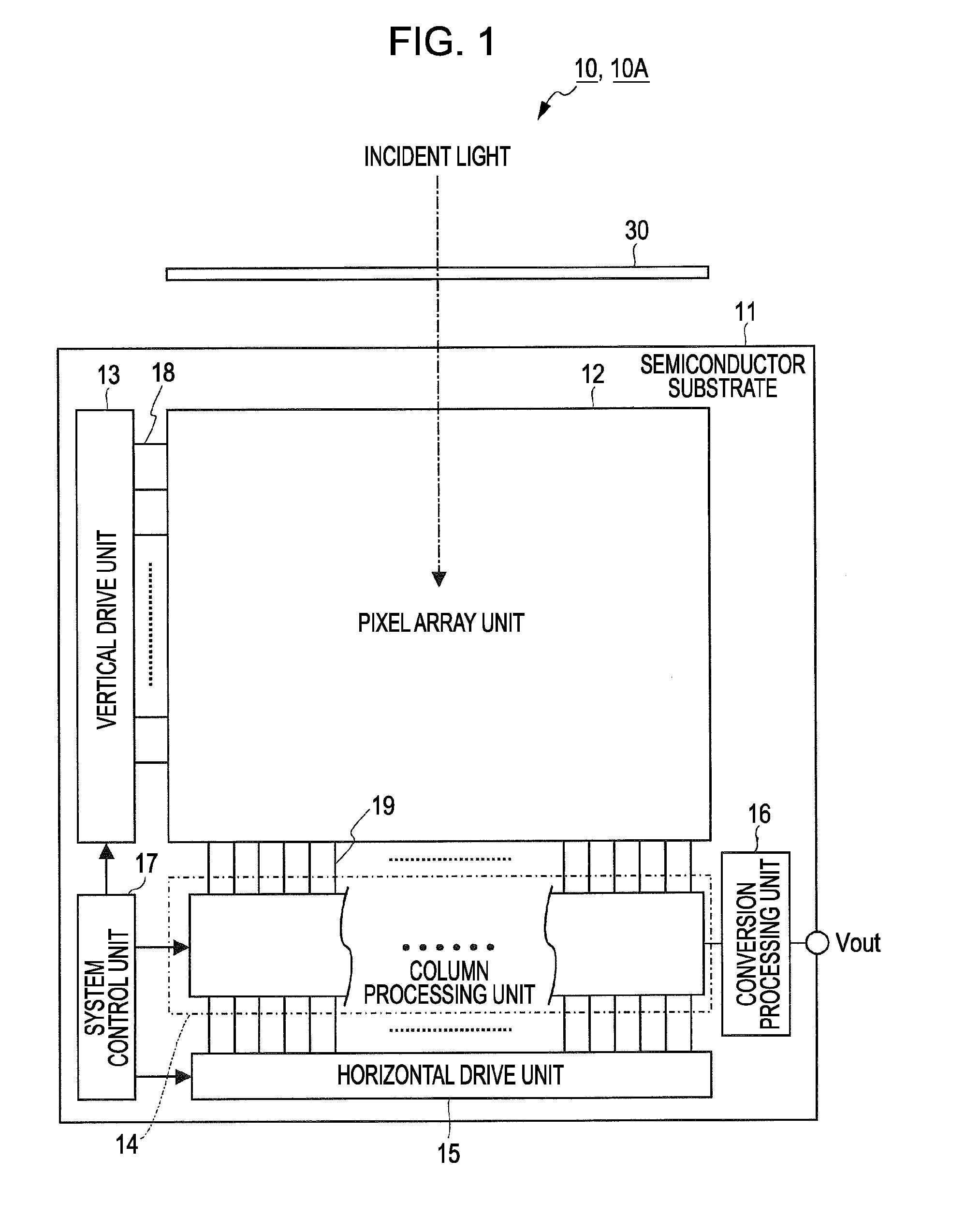
[0094]FIG. 1 is a schematic illustration of an exemplary system configuration of a solid-state imaging device (e.g., a CMOS image sensor, which is an example of an X-Y addressing solid-state imaging device) according to a first exemplary embodiment of the present invention.

[0095]According to the first embodiment, a CMOS image sensor 10 includes a semiconductor substrate (hereinafter also referred to as a “sensor chip”) 11. The sensor chip 11 includes a pixel array unit 12 formed thereon and a peripheral circuit unit integrated thereon. For example, the peripheral circuit unit includes a vertical drive unit 13, a column processing unit 14, a horizontal drive unit 15, a conversion processing unit 16, and a system control unit 17.

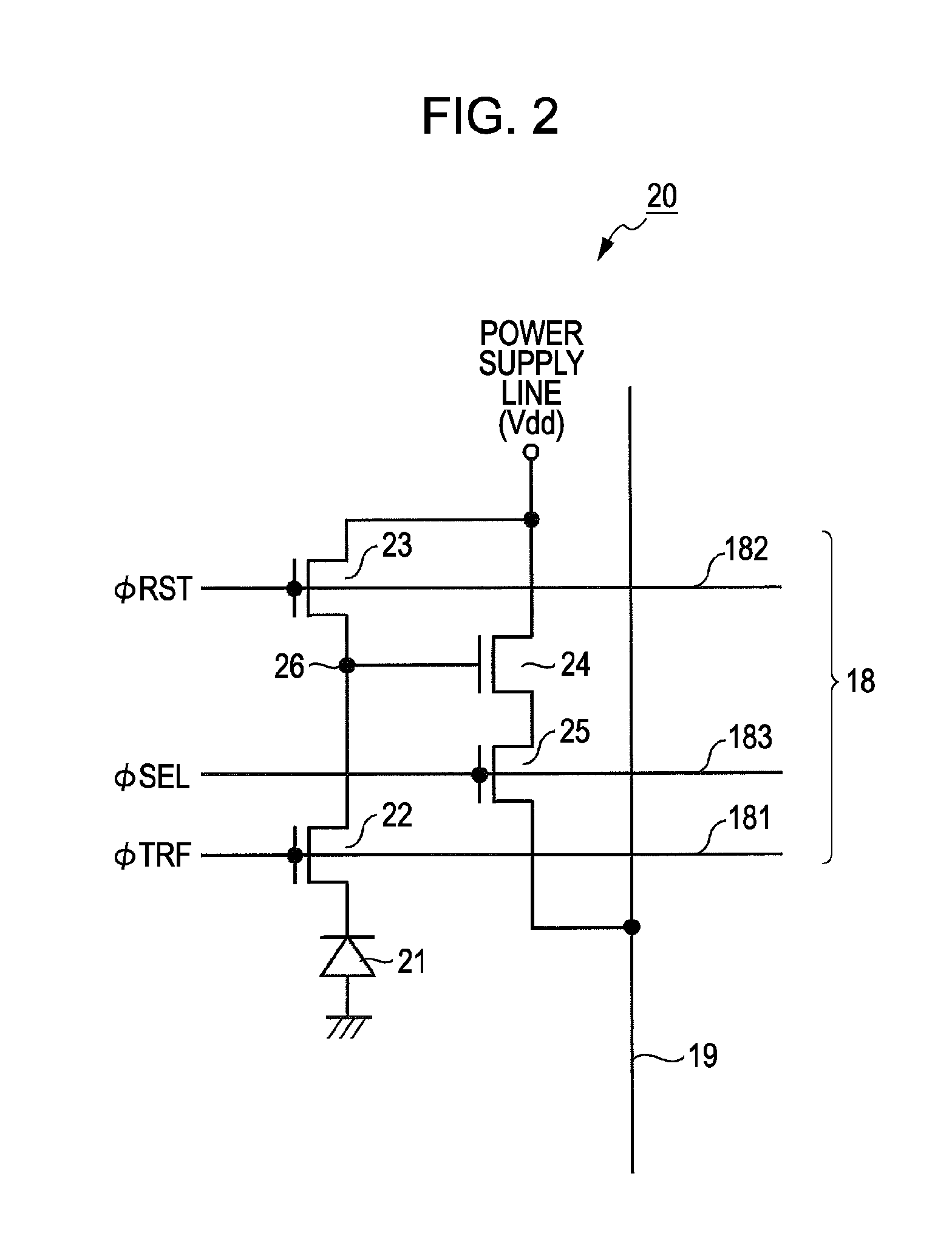
[0096]The pixel array unit 12 includes a plurality of unit pixels (not shown), each including a photoelectric conversion element, two-dimensionally arranged in an array. The unit pixel (hereinafter also sim...

first example of first exemplary embodiment

[0132]FIG. 4 is a color arrangement diagram illustrating color coding according to a first example of the first exemplary embodiment. As shown in FIG. 4, in the color coding according to the first example of the first exemplary embodiment, W filters that maximize the output level are arranged in a checkerboard pattern. R filters are arranged in a checkerboard pattern at a two-pixel pitch in the vertical direction and the horizontal direction. Similarly, B filters are arranged in a checkerboard pattern at a two-pixel pitch in the vertical direction and the horizontal direction. Each of the R filters is diagonally shifted from one of the B filters by one pixel. In addition, G filters are arranged in the other area of the checkerboard pattern.

[0133]More specifically, in a 4×4 pixel block, W filters are arranged in a checkerboard pattern. R filters are arranged in the second row and first column and in the fourth row and third column. B filters are arranged in the first row and second c...

second example of first exemplary embodiment

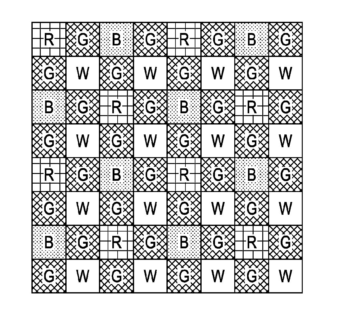
[0134]FIG. 5 is a color arrangement diagram illustrating color coding according to a second example of the first exemplary embodiment. As shown in FIG. 5, in the color coding according to the second example of the first exemplary embodiment, W filters are arranged in a checkerboard pattern. R filters are squarely arranged in the pattern at a four-pixel pitch in the vertical direction and the horizontal direction. Similarly, B filters are squarely arranged in the pattern at a four-pixel pitch in the vertical direction and the horizontal direction. In addition, each of the R filters is diagonally shifted from one of the B filters by one pixel. In addition, G filters are arranged in the other area in the checkerboard pattern.

[0135]More specifically, in a 4×4 pixel block, W filters are arranged in a checkerboard pattern. An R filter is disposed in the second row and third column. A B filter is disposed in the third row and second column. This array is the square array having a four-pixe...


PUM


Abstract

A solid-state imaging device includes a color filter unit disposed on a pixel array unit including pixels two-dimensionally arranged in a matrix and a conversion processing unit disposed on a substrate having the pixel array unit thereon. The color filter unit has a color arrangement in which a color serving as a primary component of a luminance signal is arranged in a checkerboard pattern and a plurality of colors serving as color information components are arranged in the other area of the checkerboard pattern. The conversion processing unit converts signals that are output from the pixels of the pixel array unit and that correspond to the color arrangement of the color filter unit into signals that correspond to a Bayer arrangement and outputs the converted signals.

Description

BACKGROUND OF THE INVENTION[0001]1. Field of the Invention[0002]The present invention relates to a solid-state imaging device, a method for processing a signal of the solid-state imaging device, and an imaging apparatus.[0003]2. Description of the Related Art[0004]In order to increase the sensitivity of solid-state imaging devices, a plurality of techniques in terms of a color filter array and signal processing of the color filter array have been developed (refer to, for example, Japanese Unexamined Patent Application Publication No. 2007-287891). One of the color filter arrays is a color filter array that uses a color (e.g., white (W)) serving as a primary component of a luminance signal. As color coding using a white color, white checkerboard color coding in which white is arranged in a checkerboard pattern is frequently used.[0005]The output voltage of a color filter array using a white color is higher than that of a color filter array having an RGB Bayer arrangement that has bee...

Claims


Application Information

Patent Timeline
Patent Type & Authority Applications(United States)
IPC IPC(8): H04N5/335
CPCH04N5/2254H04N9/045G06T7/90H01L27/14605H01L27/14621H01L27/14627H04N25/133H04N25/135H04N23/843G02B5/20G02B13/0015H04N9/646H04N9/77H04N25/778
Inventor HIROTA, ISAO
Owner SONY CORP
Why Eureka
Try Eureka