Semiconductor process equipment

A technology of process equipment and semiconductors, applied in semiconductor/solid-state device manufacturing, electrical components, circuits, etc., can solve problems such as time-consuming, long-term, and affecting chamber process efficiency, and achieve the effect of shortening the time used

Pending Publication Date: 2022-07-12
BEIJING NAURA MICROELECTRONICS EQUIP CO LTD
View PDF0 Cites 0 Cited by
  • Summary
  • Abstract
  • Description
  • Claims
  • Application Information

AI Technical Summary

Problems solved by technology

However, the process temperature of the PVD process is generally 200°C to 400°C, and it usually takes 6 to 8 hours to cool down to room temperature, and it takes a long time to raise the temperature in the chamber to the process temperature after the residual charge is eliminated. time; it can be seen that although the traditional method of eliminating the residual charge on the surface of the electrostatic chuck is simple, it takes a long time and seriously affects the process efficiency of the chamber

Method used


Image

  • Semiconductor process equipment
  • Semiconductor process equipment
  • Semiconductor process equipment

Examples


Embodiment Construction

[0027] In order to make those skilled in the art better understand the technical solutions of the present invention, the semiconductor process equipment provided by the present invention will be described in detail below with reference to the accompanying drawings.

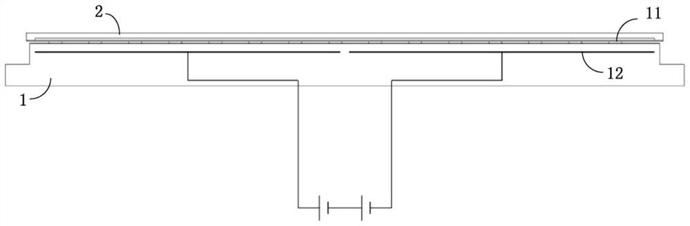
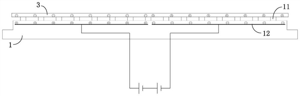
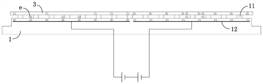
[0028] This embodiment proposes a semiconductor process equipment, including a process chamber and an electrostatic chuck disposed in the process chamber, and a plurality of bumps are provided on the bearing surface of the electrostatic chuck to support the wafer; The material usually has the characteristics of high strength and not easy to bend, so when the wafer is adsorbed on the carrier surface, the wafer only receives the support force from multiple bumps, and does not contact the non-bump area in the carrier surface, Therefore, by reducing the contact area with the bearing surface, the impact of micro particles on the wafer is reduced.

[0029] Please refer to figure 1 , the above-mentioned semiconductor pr...


PUM


Abstract

The invention provides semiconductor process equipment, which comprises a process chamber and an electrostatic chuck arranged in the process chamber, and is characterized in that a plurality of salient points are arranged on the bearing surface of the electrostatic chuck and are used for supporting a wafer; the equipment further comprises a charge eliminating device and a grounded sheet taking part. Wherein the charge eliminating device comprises an elastic conductive part, and when the elastic conductive part is placed on the plurality of salient points and when the electrostatic chuck is electrified, the elastic conductive part can generate elastic deformation under the action of electrostatic force so as to be in contact with the bearing surface of the electrostatic chuck, so that residual charges on the bearing surface are transferred; the sheet taking part is used for placing the elastic conductive part on the plurality of salient points or taking away the elastic conductive part from the plurality of salient points; and the sheet taking part is grounded. According to the semiconductor process equipment provided by the invention, the residual charge on the bearing surface of the electrostatic chuck can be quickly eliminated, and the process chamber does not need to be opened.

Description

technical field [0001] The present invention relates to the field of semiconductor manufacturing, in particular, to a semiconductor process equipment. Background technique [0002] In the PVD (Physical Vapor Deposition, physical vapor deposition) process, an electrostatic chuck is usually used to fix the wafer. At the same time, the electrostatic chuck also has the function of heating the wafer to maintain the wafer temperature at a preset process temperature until The process is over. Moreover, in order to improve the heat exchange efficiency between the electrostatic chuck and the wafer, it is necessary to pass gas between the electrostatic chuck and the wafer, and maintain a certain pressure, and realize the heat exchange between the electrostatic chuck and the wafer through the gas. . With the use of the electrostatic chuck, residual charge will accumulate on the surface of the electrostatic chuck. However, due to the uncontrollable residual charge, it is often unevenl...

Claims


Application Information

Patent Timeline
Patent Type & Authority Applications(China)
IPC IPC(8): H01L21/683
CPCH01L21/6831H01L21/6833
Inventor 于斌
Owner BEIJING NAURA MICROELECTRONICS EQUIP CO LTD
Why Eureka
Try Eureka