GaN-based LED epitaxial structure, preparation method thereof and light-emitting diode

An epitaxial structure, methyl gallium technology, applied in semiconductor devices, electrical components, circuits, etc., can solve the problems of decreasing the luminous efficiency of light-emitting diodes, increasing the resistivity of P-type GaN, increasing the forward voltage of light-emitting diodes, etc. The effect of reducing content, reducing resistivity and easy cracking

Pending Publication Date: 2022-07-29
HUAIAN AUCKSUN OPTOELECTRONICS TECHNOLOGY CO LTD
View PDF5 Cites 1 Cited by
  • Summary
  • Abstract
  • Description
  • Claims
  • Application Information

AI Technical Summary

Problems solved by technology

[0003] In practical application, the existing technology has at least the following problems: in the low-temperature P-type GaN layer, due to the growth and formation of trimethylgallium, the content of carbon impurities in it is relatively high, and the carbon impurities may form donors in the P-type GaN, thereby compensating The acceptor increases the resistivity of P-type GaN, which in turn increases the forward voltage of the light-emitting diode, resulting in a decrease in the luminous efficiency of the light-emitting diode

Method used


Image

  • GaN-based LED epitaxial structure, preparation method thereof and light-emitting diode
  • GaN-based LED epitaxial structure, preparation method thereof and light-emitting diode
  • GaN-based LED epitaxial structure, preparation method thereof and light-emitting diode

Examples


Embodiment approach 1

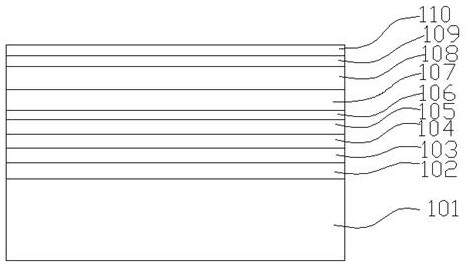
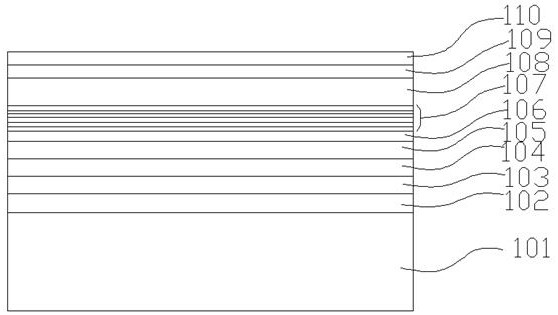
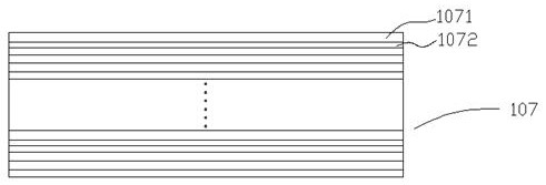
[0021] This embodiment provides a GaN-based LED epitaxial structure, such as figure 2 As shown, it includes a substrate, and a buffer layer, a uGaN layer, an nGaN layer, a stress release layer, a quantum well layer, a low temperature pGaN layer, a pALGaN layer, a pGaN layer and a contact layer grown on the substrate in sequence; the low temperature pGaN layer From a trimethylgallium sublayer with a carbon impurity content of 8.0E16 and a carbon impurity content of 2.0E16 Atoms / cm 3 The triethylgallium sublayers are alternately grown for 10 cycles to form. In the low temperature pGaN layer, the total thickness of the trimethylgallium sublayer is 10 nm, and the total thickness of the triethylgallium sublayer is also 10 nm.

[0022] The preparation method of the above-mentioned GaN-based LED epitaxial structure is as follows:

[0023] Step 1, heating the ALN-plated pss substrate 101 to 1000-1200° C. for surface cleaning treatment for 5-10 minutes;

[0024] Step 2, reducing th...

Embodiment approach 2

[0035] This embodiment is exactly the same as Embodiment 1, except that the carbon impurity content of the triethylgallium sublayer in this embodiment is 3.0E16 Atoms / cm 3 .

Embodiment approach 3

[0037] This embodiment is exactly the same as Embodiment 1, except that the carbon impurity content of the triethylgallium sublayer in this embodiment is 5.0E16 Atoms / cm3 .


PUM

PropertyMeasurementUnit
thicknessaaaaaaaaaa
thicknessaaaaaaaaaa

Abstract

The invention relates to the field of semiconductors, and discloses a GaN-based LED epitaxial structure, a preparation method thereof and a light emitting diode, the epitaxial structure comprises a substrate (101), and an nGaN layer (104), a quantum well layer (106) and a pGaN layer (109) which grow on the substrate in sequence; a low-temperature pGaN layer (107) also grows between the quantum well layer and the pGaN layer, and the low-temperature pGaN layer is formed by alternately growing a trimethyl gallium sub-layer (1071) with relatively high carbon impurity content and a triethyl gallium sub-layer (1072) with relatively low carbon impurity content. Compared with the prior art, the low-temperature PGaN layer is formed in the mode that the trimethyl gallium and the triethyl gallium alternately grow, the content of carbon impurities in the low-temperature PGaN layer is reduced, the resistivity of the low-temperature PGaN is reduced, the forward voltage of the light-emitting diode is further reduced, and the light-emitting efficiency of the light-emitting diode is improved.

Description

technical field [0001] The invention relates to the field of semiconductors, in particular to a GaN-based LED epitaxial structure, a preparation method thereof, and a light-emitting diode. Background technique [0002] A GaN (gallium nitride)-based LED (Light Emitting Diode) generally includes an epitaxial wafer and electrodes prepared on the epitaxial wafer. like figure 1 As shown, the epitaxial wafer generally includes: a substrate, and a GaN-based epitaxial layer grown on the substrate, the epitaxial layer includes a buffer layer, an undoped GaN layer, an N-type GaN layer, a stress release layer, and a quantum well stacked in sequence layer, low temperature P-type GaN layer, PAlGaN layer, P-type GaN layer and contact layer. When a current is injected into the GaN-based LED, electrons in the N-type region such as the N-type GaN layer and holes in the P-type region such as the P-type GaN layer enter the active region of the quantum well layer and recombine, emitting visib...

Claims


Application Information

Patent Timeline
Patent Type & Authority Applications(China)
IPC IPC(8): H01L33/14H01L33/06H01L33/32H01L33/00
CPCH01L33/14H01L33/06H01L33/32H01L33/0075
Inventor 展望宋长伟刘康张雷城芦玲
Owner HUAIAN AUCKSUN OPTOELECTRONICS TECHNOLOGY CO LTD
Why Eureka
Try Eureka