Connection structure of CMOS double-row DUP and internal ESD device

A technology of ESD devices and connection structures, applied in semiconductor devices, electric solid devices, electrical components, etc., can solve problems such as waste and achieve the effect of improving utilization

Pending Publication Date: 2022-08-02
珠海鸿芯科技有限公司
View PDF0 Cites 0 Cited by
  • Summary
  • Abstract
  • Description
  • Claims
  • Application Information

AI Technical Summary

Problems solved by technology

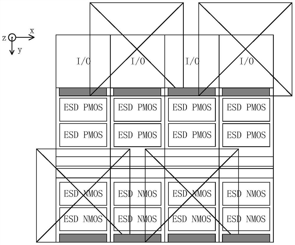
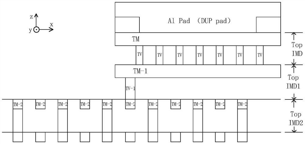
[0007] It can be seen from the above scheme that the present invention solves the problem of waste of space on the height of the chip corresponding to this part of the area when the area of ​​the PAD exceeds a part of the GPIO area by setting the second metal interface between the two ESD PMOS tubes arranged side by side up and down. problem, so that the double-row PAD can all fall on the top of the GPIO, improving the utilization of the chip area

Method used


Image

  • Connection structure of CMOS double-row DUP and internal ESD device
  • Connection structure of CMOS double-row DUP and internal ESD device
  • Connection structure of CMOS double-row DUP and internal ESD device

Examples


Embodiment Construction

[0019] In the present invention, in the connection between the double-row DUP and the internal ESD device, a second metal interface is arranged between two ESD PMOS transistors arranged side by side up and down.

[0020] In the present invention, "first", "second" and "third" are all used to distinguish similar things, and have no meaning of order. The height mentioned in the present invention refers to the direction along the z-axis, and the width refers to the direction of the x-axis.

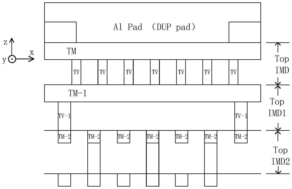
[0021] see image 3 , the metal layer of the PAD includes a TM layer and a TM-1 layer, the TM layer and the TM-1 layer are connected through a first through silicon via TV, and the TM-1 layer and another metal layer TM-2 layer are connected through a second Through silicon via TV-1 connection. The lowest metal layer of the PAD is the TM-1 layer, and the TM-2 layer is the device area, where the GPIO (not shown in the figure) is placed. IMD (inter metaldielectric) is a metal internal dielect...


PUM


Abstract

The invention provides a CMOS double-row DUP and internal ESD device connection structure, which comprises double PADs and a plurality of GPIOs, the lowest layer metal of each PAD in the double-row PADs is connected with the GPIO, the GPIO comprises an I/O port and an ESD device, the ESD device and the I/O port are sequentially arranged from inside to outside along a circuit layout, and the I/O port is connected with the ESD device; the ESD device comprises two ESD PMOS (P-channel Metal Oxide Semiconductor) tubes arranged side by side up and down and two ESD NMOS (N-channel Metal Oxide Semiconductor) tubes arranged side by side up and down, and the two ESD PMOS tubes arranged side by side up and down are arranged above the two ESDNMOS tubes arranged side by side up and down; a first metal interface is arranged below the two ESD NMOS transistors which are arranged side by side up and down, and a second metal interface is arranged between the two ESD PMOS transistors which are arranged side by side up and down; the bottommost metal of the PAD is connected with the first metal interface or the second metal interface, the problem that the area of the PAD exceeds a part of the area of the GPIO, so that the space in the height of a chip corresponding to the part of the area is wasted can be solved, and the utilization rate of the area of the chip is increased.

Description

technical field [0001] The invention relates to the field of integrated circuit design, in particular to a connection structure between a CMOS double-row DUP and an internal ESD device. Background technique [0002] In integrated circuits, layout design is generally considered as a compromise between performance, area, and time. However, in the early layout planning stage, on the basis of ensuring performance, area is particularly important. [0003] In a specific design, ESD (Electro-Static discharge) devices and PAD (pads) occupy a large area in the layout. In the DUP (Device Under Pad) structure, the ESD device or other device is placed under the PAD, which makes reasonable use of the layout area. [0004] DUP structure reference under existing CMOS process design rules figure 1 , refer to the schematic diagram of the connection layout of the double-row DUP and the internal ESD device figure 2 , with the up-down direction as the reference, the device and the PAD are t...

Claims


Application Information

Patent Timeline
Patent Type & Authority Applications(China)
IPC IPC(8): H01L27/02H01L27/092
CPCH01L27/0207H01L27/0251H01L27/0292H01L27/092
Inventor 茹金泉陈明瑜陈永烈陈明娇
Owner 珠海鸿芯科技有限公司
Why Eureka
Try Eureka