
Small-sized image pickup module

A camera module, a small technology, applied in image communication, radiation control devices, instruments, etc., can solve the problems of increased manufacturing cost, complex structure, and poor productivity

Inactive Publication Date: 2005-03-16
OLYMPUS OPTICAL CO LTD
View PDF4 Cites 0 Cited by
  • Summary
  • Abstract
  • Description
  • Claims
  • Application Information

AI Technical Summary

Problems solved by technology

[0022] However, in such a structure, a lens cap and a guide pin are required, the structure is complicated, and there are problems in that the productivity is lowered and the manufacturing cost is increased.
[0023] That is, in the above-mentioned conventional solid-state imaging device, the size of the steps between the positioning parts is prone to error, the management of the size is difficult, and the positional accuracy of the lens with respect to the solid-state imaging element in the optical axis direction cannot be sufficiently ensured.
[0024] Furthermore, in the above-mentioned conventional solid-state imaging device, the structure is complicated, the productivity thereof deteriorates, and the manufacturing cost increases, so it becomes an expensive product.

Method used


Image

  • Small-sized image pickup module
  • Small-sized image pickup module
  • Small-sized image pickup module

Examples


no. 1 example

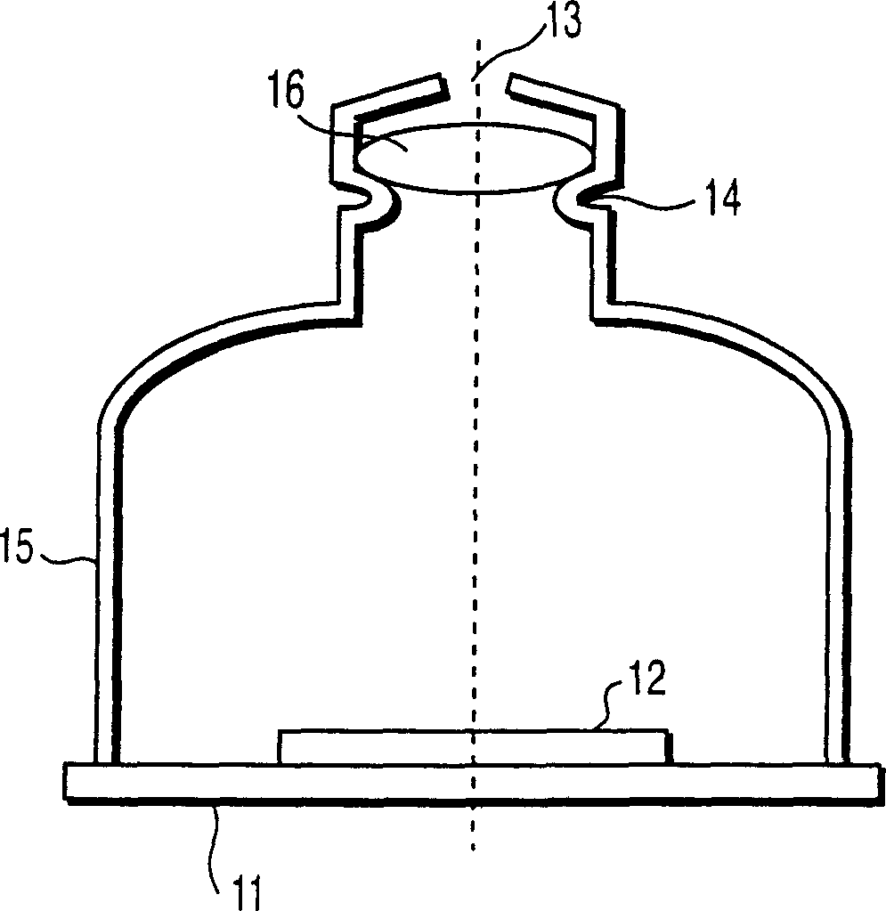
[0078] figure 1 It is a cross-sectional view showing a schematic configuration of the compact camera module according to the first embodiment of the present invention.

[0079] That is, if figure 1 As shown, the small camera module of the first embodiment of the present invention, as its basic structure, includes: a non-metallic substrate 11 including ceramics and the like; A semiconductor device chip 12 for imaging such as a C-MOS image sensor; a mirror frame body 15, in which the semiconductor device chip 12 for imaging is accommodated, is mounted on the basis of the above-mentioned non-metal substrate 11, from its top The part is sequentially integrally punched and formed with an aperture part 13 and a lens fixing part 14;

[0080] Here, in the semiconductor device chip 12 for imaging, a semiconductor circuit portion and the like are provided, and the semiconductor circuit portion is formed on the same semiconductor chip by, for example, a two-dimensional arrangement cons...

no. 2 example

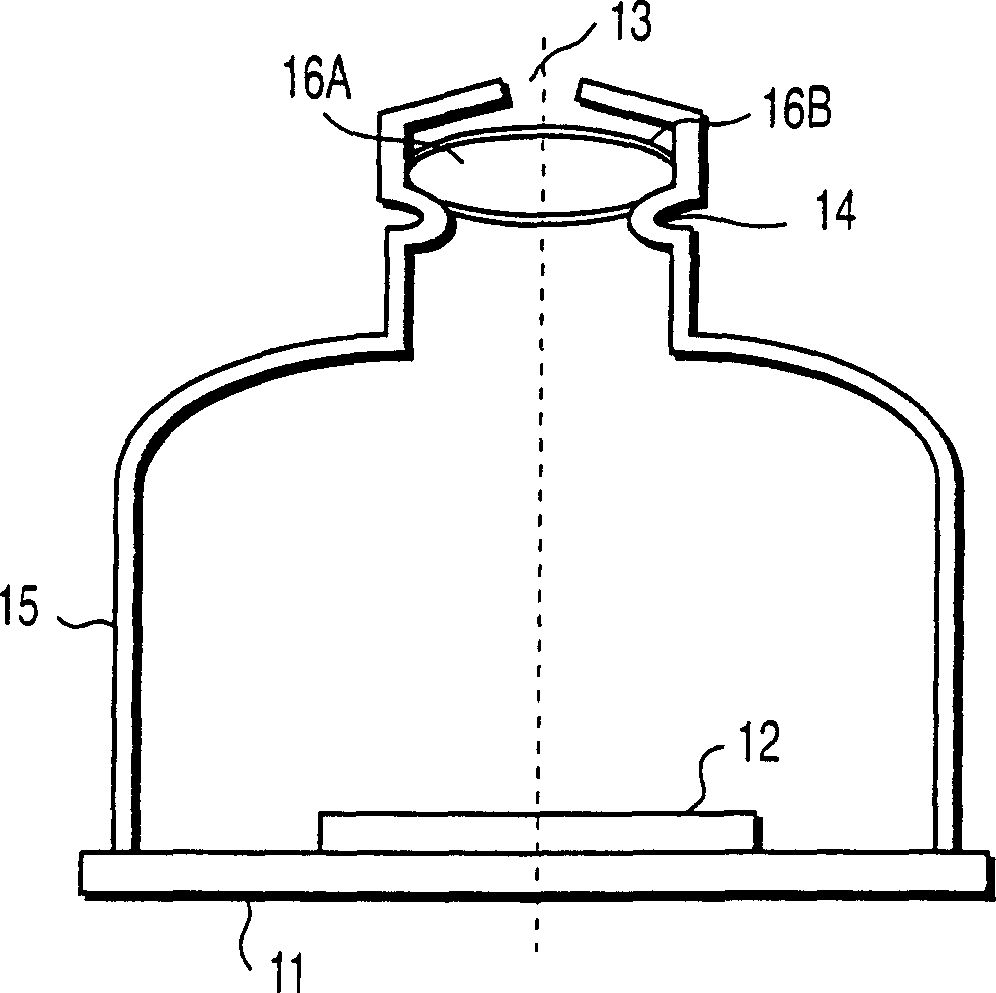
[0089] figure 2 It is a cross-sectional view showing a schematic configuration of a small camera module according to a second embodiment of the present invention.

[0090] That is, if figure 2 As shown, the small camera module of the second embodiment of the present invention, as its basic structure, includes: a non-metallic substrate 11 including ceramics and the like; A semiconductor device chip 12 for imaging such as a C-MOS image sensor; a mirror frame body 15, which contains the semiconductor device chip 12 for imaging, is mounted on the basis of the above-mentioned non-metallic substrate as 11, from which The top end part is sequentially integrally stamped with an aperture part 13 and a lens fixing part 14 ; and a lens 16A mounted on the lens fixing part 14 of the mirror frame body 15 .

[0091] In this case, the feature is that the lens 16A attached to the lens fixing portion 14 of the lens frame body 15 doubles as an infrared shielding filter by applying an infrare...

no. 3 example

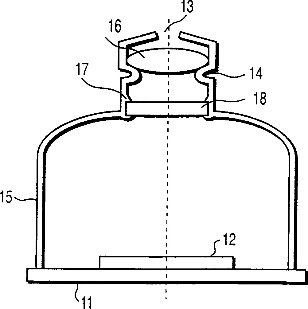
[0102] image 3 It is a sectional view showing a schematic configuration of a small camera module according to a third embodiment of the present invention.

[0103] That is, if image 3 As shown, the small camera module of the third embodiment of the present invention, as its basic structure, includes: a non-metallic substrate 11 including ceramics and the like; A semiconductor device chip 12 for imaging such as a C-MOS image sensor; a mirror frame body 15, which contains the semiconductor device chip 12 for imaging, is mounted on the basis of the above-mentioned non-metallic substrate as 11, from which The top end portion is sequentially integrally stamped with an aperture portion 13, a lens fixing portion 14, and an infrared shading filter fixing portion 17; the lens 16 mounted on the lens fixing portion 14 of the above-mentioned mirror frame body 15; and, being mounted on the mirror frame The infrared light shielding filter 18 on the infrared light shielding filter fixing...


PUM


Abstract

The present invention provides a small image pickup module in which a structure, which mounts a lens-barrel body so as to enclose therein a semiconductor device chip for image pickup mounted on a substrate, is improved, and in which assembly work is easy and a reduction in costs is possible. In accordance with one aspect of the present invention, there is provided a small image pickup module comprising a substrate made from a nonmetal including a ceramic or the like, a semiconductor device chip for image pickup including a two-dimensional C-MOS image sensor or the like which is mounted to the substrate, a lens-barrel body which is attached as a reference on the substrate so as to enclose the semiconductor device chip for image pickup therein, and in which a diaphragm section and a lens fixing portion are press-formed integrally in that order from the distal end portion, and a lens which is mounted to the lens fixing portion of the lens-barrel body.

Description

technical field [0001] The present invention relates to a small camera module, in particular to an integrated small camera module in which a lens and a semiconductor device chip for camera are accommodated in one package. Background technique [0002] In recent years, in various multimedia fields such as notebook personal computers and mobile phones, as well as in image input devices such as information terminals such as surveillance cameras and video tape recorders, and in-vehicle applications, small image sensors The demand for units is constantly increasing. [0003] A small image sensor unit suitable for such an image input device is an integrated camera module in which parts such as a solid-state imaging element, a lens unit, a filter, and an aperture unit are housed in one package. [0004] A camera module as a conventional image sensor unit has a structure in which a solid-state imaging element is mounted on a substrate, and then the substrate is fixed in an assembly...

Claims


Application Information

Patent Timeline
Patent Type & Authority Patents(China)
IPC IPC(8): H01L27/14G02B7/02H01L27/146H01L31/0203H01L31/0232H04N25/00
CPCG02B7/02H01L27/14625H01L31/0203H01L27/14618H04N5/2254H01L31/0232H04N5/2253H01L2924/0002H01L31/02325H01L27/14643H04N23/55H04N23/54H01L2924/00H01L27/14
Inventor 中城泰生
Owner OLYMPUS OPTICAL CO LTD
Learn More