Plane switch mode active matrix liquid crystal display device and mfg. method thereof

An active matrix, planar switch technology, used in static indicators, instruments, transistors, etc., can solve problems such as not being able to completely shield and reduce the impact of light

Inactive Publication Date: 2005-06-22
NEC LCD TECH CORP
View PDF10 Cites 1 Cited by
  • Summary
  • Abstract
  • Description
  • Claims
  • Application Information

AI Technical Summary

Problems solved by technology

[0022] However, the conventional liquid crystal display devices proposed by the above-mentioned published patents are accompanied by the inability to completely shield and reduce the effects of the reduction of light caused by the use of a common electrode comprising a light-impermeable material.

Method used


Image

  • Plane switch mode active matrix liquid crystal display device and mfg. method thereof
  • Plane switch mode active matrix liquid crystal display device and mfg. method thereof
  • Plane switch mode active matrix liquid crystal display device and mfg. method thereof

Examples


no. 1 approach

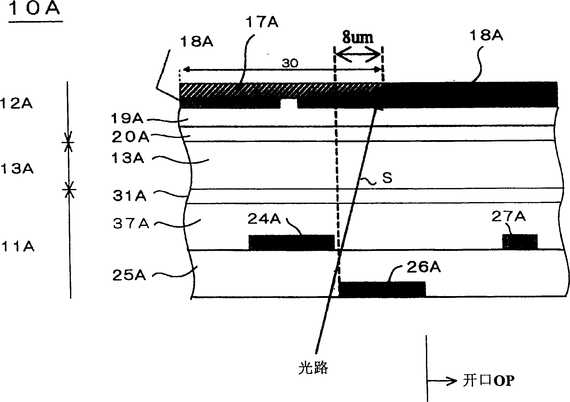
[0307] Figure 4 , 5 and 6 exemplify the planar switching mode active matrix type liquid crystal display device employed based on the first embodiment of the present invention. Figure 4 is a plan view of the liquid crystal display device 10 employed based on the first embodiment, Figure 5 is in Figure 4 The sectional view taken along the V-V line in the middle, and at the same time Image 6 is a circuit diagram of a unit pixel.

[0308] Such as Figure 5 As shown, the liquid crystal display device 10 is composed of an active device substrate 11 , an opposite substrate 12 and a liquid crystal layer 13 interposed between the active device substrate 11 and the opposite substrate 12 .

[0309] The opposing substrate 12 includes an electrically insulating transparent substrate 16, a black matrix layer 17 formed on the first surface of the electrically insulating transparent substrate 16 as an opaque film, and a colored layer formed on the first surface of the electrically i...

no. 1 example

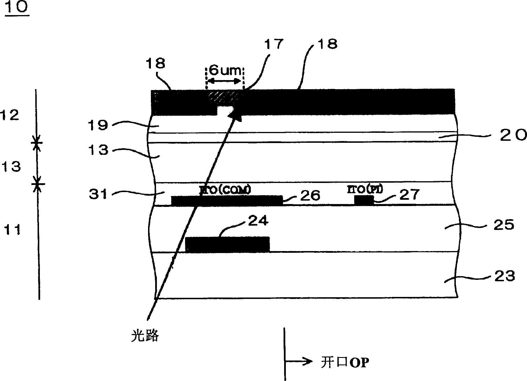
[0430] 28A to 28K are sectional views of the liquid crystal display device 10 showing steps of a first example of the method of manufacturing the liquid crystal display device 10 including the second interlayer insulating film 25 having a multilayer structure of inorganic films and organic films.

[0431] First, as shown in FIG. 28A, a chromium layer as a first metal layer is formed on a glass substrate as an electrically insulating transparent substrate 22, and then, the chromium layer is made into a gate 30c and a common electrode by photolithography and dry etching. The pattern of lines 26a and 26b. Although only the common electrode line 26b is shown in FIGS. 28A to 30I, the common electrode line 26a will be described below together with the common electrode line 26b because the common electrode line 26a is formed together with the common electrode line 26b.

[0432] Then, as shown in FIG. 28B, a first interlayer insulating film 23 is formed over the entire transparent sub...

no. 2 example

[0443] 29A to 29I are cross-sectional views of the liquid crystal display device 10 showing steps of a second example of the method of manufacturing the liquid crystal display device 10 including the second interlayer insulating film 25 composed of a single organic film.

[0444] First, as shown in FIG. 29A, a chromium layer as a first metal layer is formed on a glass substrate as an electrically insulating transparent substrate 22, and then, the chromium layer is formed into a gate 30c and a common electrode by photolithography and dry etching. The pattern of lines 26a and 26b.

[0445] Then, as shown in FIG. 29B, the first interlayer insulating film 23 is formed over the entire transparent substrate 22, covering the gate electrode 30c and the common electrode lines 26a and 26b. The first interlayer insulating film 23 has a multilayer structure composed of a silicon dioxide (SiO2) film and a silicon nitride (SiNx) film.

[0446] Then, as shown in FIG. 29C , an amorphous sili...


PUM

PropertyMeasurementUnit
thicknessaaaaaaaaaa
widthaaaaaaaaaa
widthaaaaaaaaaa

Abstract

A planar switching mode active matrix liquid crystal display device, comprising a first substrate (11), a second substrate (12) opposite to the first substrate, and a liquid crystal layer (13) sandwiched between the first and second substrates ). The first substrate includes thin film transistors, pixel electrodes (27), common electrodes (26), data lines, scanning lines and common electrode lines respectively related to the pixels to be driven. The axes of the liquid crystal molecules are rotated on a plane parallel to the first substrate by means of an electric field substantially parallel to the plane of the first substrate, so as to display a certain image. The common electrode (26) is made of a transparent material and is formed closer to the liquid crystal layer than the data lines. The common electrode (26) completely overlaps the data line (24) except in the area of ​​the data line located near the scan line. The liquid crystal display device further includes an opaque layer (17) in the area where the common electrode completely overlaps the data line, the opaque layer is formed by the black matrix layer (17), and its width is smaller than that of the common electrode.

Description

technical field [0001] The invention relates to a liquid crystal display device and its manufacturing method, in particular to a planar switch mode active matrix liquid crystal display device and its manufacturing method. Background technique [0002] Liquid crystal display devices can be divided into two types, one of which is that the molecular axis of the oriented liquid crystal molecules rotates on a plane perpendicular to the substrate to display an image; the other type is that the molecular axes of the oriented liquid crystal molecules rotate in parallel Rotate on the plane of the substrate to display an image. [0003] A standard mode in the former type is a twisted nematic (TN) mode liquid crystal display device, and the latter type is called an in-plane switching (IPS) mode liquid crystal display device. [0004] Because the viewer only watches from the direction extending along the short axis of the liquid crystal molecules, even if he / she moves the viewpoint, ho...

Claims


Application Information

Patent Timeline
Patent Type & Authority Patents(China)
IPC IPC(8): G02F1/133G02F1/1337G02F1/1343G02F1/136H01L29/786
Inventor 西田真一松本公一半贯贵久板仓州优
Owner NEC LCD TECH CORP
Why Eureka
Try Eureka