Process for producing light-emitting and/or light-receiving semiconductor body

A semiconductor and body technology, applied in the field of semiconductor body manufacturing for light emission and/or reception, to reduce the risk of detachment and improve the bonding strength

Inactive Publication Date: 2005-11-16
OSRAM GMBH
View PDF2 Cites 1 Cited by
  • Summary
  • Abstract
  • Description
  • Claims
  • Application Information

AI Technical Summary

Problems solved by technology

However, a disadvantage of such a semiconductor body is that only a part of the light generated by the semiconductor body is coupled out of the semiconductor body

Method used


Image

  • Process for producing light-emitting and/or light-receiving semiconductor body
  • Process for producing light-emitting and/or light-receiving semiconductor body
  • Process for producing light-emitting and/or light-receiving semiconductor body

Examples


Embodiment Construction

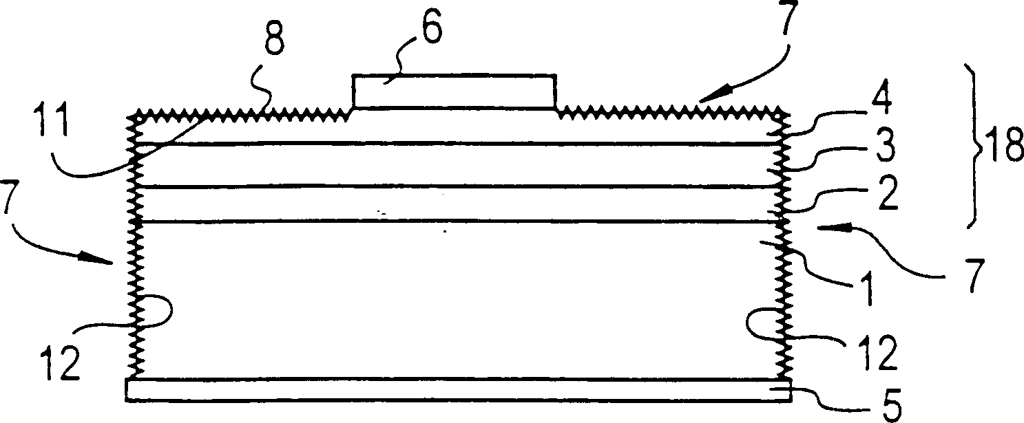
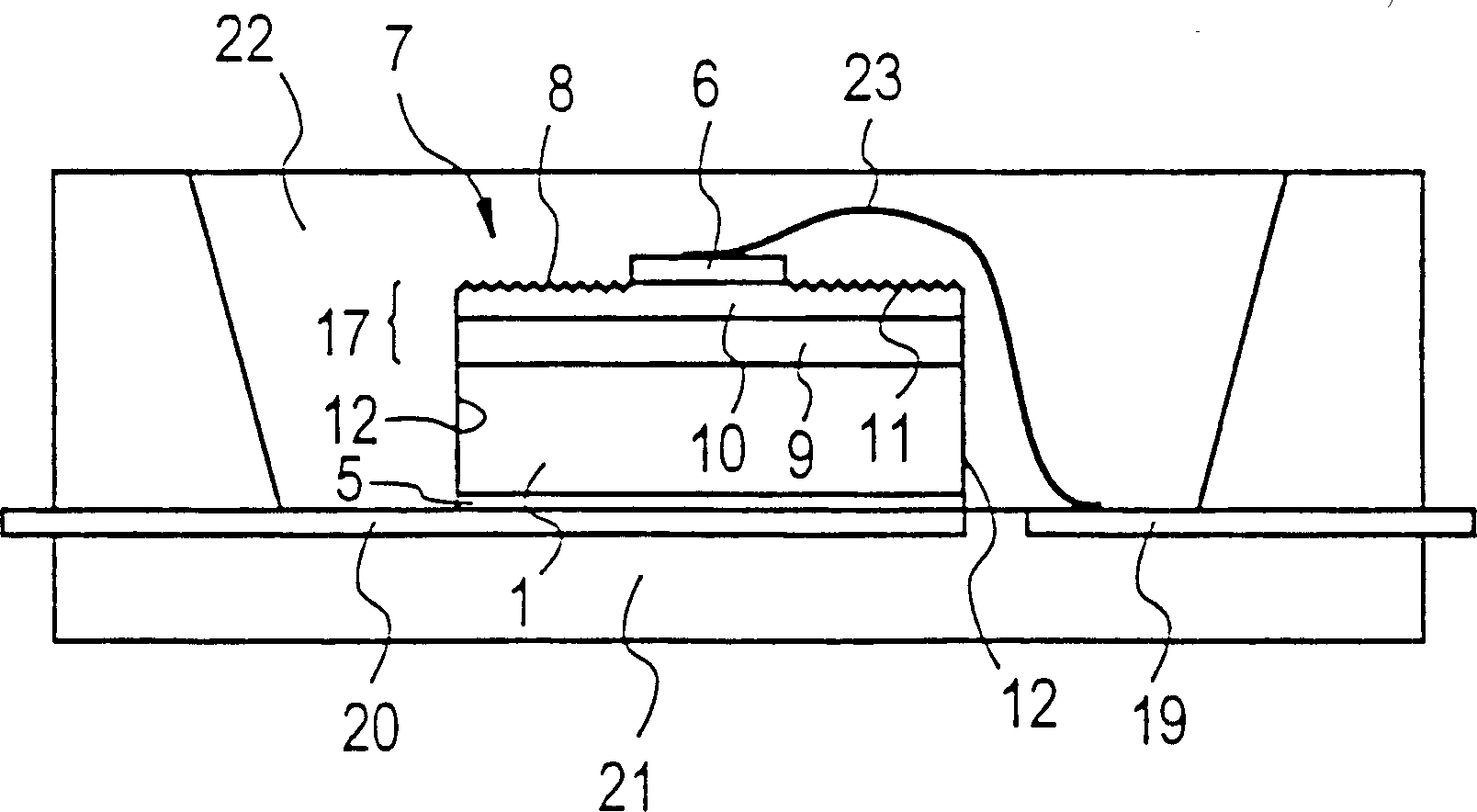
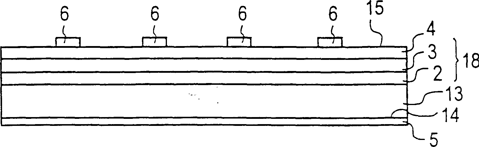
[0044] figure 1 The illustrated semiconductor body is a light-emitting semiconductor body, such as a light-emitting diode semiconductor body. In this case, a light-emitting layer sequence 18 is arranged on the GaP substrate 1 . On the GaP substrate 1 is, for example, a first GaAs x P 1-X Epitaxial layer 2, where 0≤xx P 1-X Epitaxial layer 3, where 0≤x<1. For example, Te or S can be used as n-type dopant material.

[0045] In the second GaAs x P 1-X The epitaxial layer 3 is coated with p-doped third GaAs x P 1-X The epitaxial layer 4, where 0≤xx P 1-X The epitaxial layer 2 has an increased As content, such as from x=0 until x=second GaAs x P 1-X As content of the epitaxial layer 4.

[0046] The bottom surface of the GaP substrate 1 is configured with a first contact metallization layer 5, which includes a layer sequence such as Au—Ge alloy / Ag / Au. In the third GaAs x P 1-X The top surface of the epitaxial layer 4 is configured with a second contact metallization l...


PUM


Abstract

This invention concerns a process for producing a light-emitting and/or receiving semiconductor body with at least one semiconductor layer which consists of GaAsxP1-x with 0 <= X < 1. According to the process in the invention, at least one part of the surface of the semiconductor layer is treated in a first etching step with an etching solution composed of H2SO4:H2O2:H2O and, subsequently, in a second etching step with hydrofluoric acid to produce roughness on that at least part of the semiconductor layer surface.

Description

technical field [0001] The invention relates to a method for producing a light emitting and / or receiving semiconductor body having at least one layer made of GaAs x P 1-X Composed of semiconductor layers, where 0≤x<1. Background technique [0002] Several light-emitting diodes with such semiconductor bodies are known. Thus, for example, a light-emitting diode chip is described in European Patent Registration EP 584 599, in which an n-conducting GaP epitaxial layer is applied on an n-conducting GaP substrate, and on this layer is deposited The upper p-conductive GaP epitaxial layer. The bottom surface of the GaP substrate is equipped with an antenna metallization layer composed of Au-Ge-alloy, and an antenna metallization layer is applied on the top surface of the p-GaP epitaxial layer, which consists of, for example, an Au layer, an Au-Zn layer , Ti-W-N-layer and Au or Al layer layer by layer composed of p-conductive GaP epitaxial layer. [0003] In addition, light-e...

Claims


Application Information

Patent Timeline
Patent Type & Authority Patents(China)
IPC IPC(8): H01L31/02H01L31/0236H01L33/02
CPCH01L2224/32245H01L2224/48091H01L33/025H01L2924/0002H01L31/0236H01L2224/73265H01L2224/48247Y02E10/50H01L31/02363H01L2924/00014H01L2924/00012H01L2924/00
Inventor H·菲舍尔E·尼尔施尔W·维格莱特
Owner OSRAM GMBH
Why Eureka
Try Eureka