Address generating circuit

An address generation, circuit technology, used in electrical components, electronic switches, static memory, etc.

Inactive Publication Date: 2006-02-08
FUJITSU SEMICON LTD
View PDF1 Cites 0 Cited by
  • Summary
  • Abstract
  • Description
  • Claims
  • Application Information

AI Technical Summary

Problems solved by technology

As a result, even if the fuse is in the cut state, there will be such a problem that an address corresponding to the non-cut state of the fuse will be generated due to erroneous data latching of the fuse cut information.

Method used


Image

  • Address generating circuit
  • Address generating circuit
  • Address generating circuit

Examples


no. 1 example

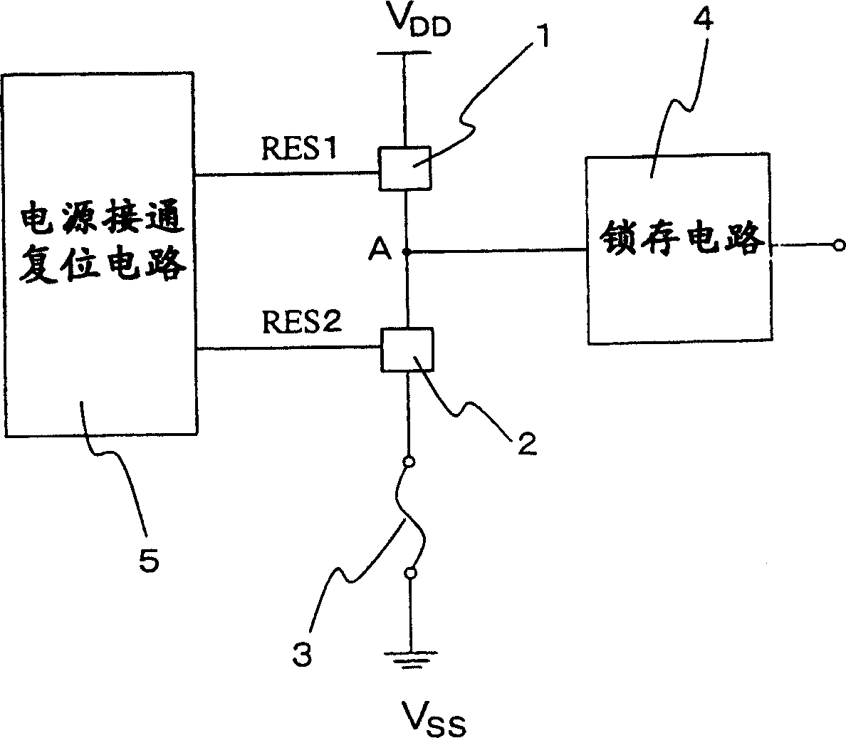
[0048] FIG. 3 is a schematic diagram of an address generation circuit according to the first embodiment of the present invention.

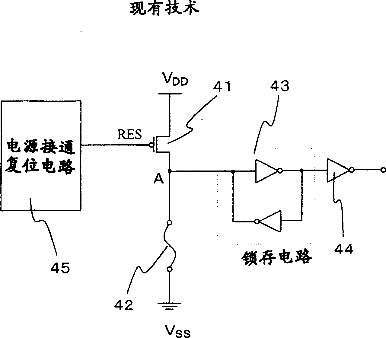
[0049] FIG. 3(a) is a circuit diagram of an address generating circuit according to a first embodiment of the present invention. In this figure, reference numeral 11 is a PMOS transistor; reference numeral 12 is an NMOS transistor; reference numeral 13 is a fuse element; reference numeral 14 is a latch circuit; An inverter; reference numeral 16 is a second inverter forming a latch circuit; reference numeral 17 is a third inverter; and reference numeral 18 is a power-on reset circuit.

[0050] In Fig. 3(a), the PMOS transistor 11, the NMOS transistor 12 and the fuse element 13 are under power supply V DD and ground V SS sequentially connected in series. The latch circuit 14 includes a first inverter 15 and a second inverter 16, the input terminal of one inverter is connected to the output terminal of the other inverter. A connection node A of t...

no. 2 example

[0074] Figure 4 is a schematic diagram of the address generating circuit of the second embodiment of the present invention. The second embodiment of the present invention provides a circuit example of the power-on reset circuit in the first embodiment.

[0075] In this figure, elements disclosed in FIG. 3 are denoted by the same reference numerals. Further, reference numeral 19 is an inverter; reference numeral 20 is a transistor whose source and drain are connected; reference numeral 21 is a PMOS transistor; and reference numeral 32 is an inverter delay circuit.

[0076] like Figure 4 As shown, the power-on reset circuit 18 of the second embodiment has a structure including two PMOS transistors 21 whose sources and drains are connected to each other and are connected in parallel between the power supply VDD and the ground VSS. . A PMOS transistor with its gate connected to its drain forms a diode transistor.

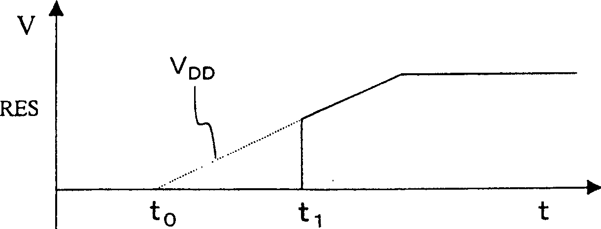
[0077] Furthermore, the power-on reset circuit 18 has a con...

no. 3 example

[0092] Figure 5 is a schematic diagram of the address generating circuit of the third embodiment of the present invention. In this figure, something like figure 2 Disclosed elements are denoted by the same reference numerals. In addition, reference numeral 22 is a first power-on reset circuit; reference numeral 23 is a second power-on reset circuit; reference numeral 24 is an NMOS transistor with a low threshold; and reference numeral 25 is an NMOS transistor with a high threshold. The transistor and reference numeral 26 is a PMOS transistor.

[0093] The address generating circuit of the third embodiment of the present invention has a structure substantially similar to that of the first and second embodiments. However, the address generation circuit of the third embodiment is different in the structure of the power-on reset circuit.

[0094] like Figure 5 As shown, the power-on reset circuit of the third embodiment includes a first power-on reset circuit 22 for outputt...


PUM


Abstract

An address generating circuit having: a first switch transistor, a second switch transistor, a fuse element, and a power-ON reset circuit for outputting a first reset signal for controlling ON / OFF conditions of the first switch transistor and a second reset signal for controlling ON / OFF conditions of the second switch transistor. The address generating circuit also includes a latch circuit for latching and outputting a predetermined potential corresponding to a cut-off or a no cut-off condition of the fuse element. The first reset signal turns ON the first switch transistor during a first period immediately after the power supply is turned ON and always holds the first switch transistor in the OFF condition after the first period is completed. Furthermore, the second reset signal turns ON the second switch transistor at least during a second period after the first period and always holds the second switch transistor in the OFF condition after the second period is completed.

Description

technical field [0001] The present invention relates to a kind of address generating circuit, especially a kind of redundant address generating circuit, is used for storing the address (hereinafter referred to as redundant address) of the damaged storage unit in a RAM (random access memory) storage unit array and in RAM A redundant address is generated when the power of the device is turned on. Background technique [0002] For example, 1(a) and 1(b) are schematic diagrams of traditional address generating circuits. [0003] FIG. 1(a) is a circuit diagram illustrating a conventional address generation circuit. In this figure, 41 is a first switching transistor including a PMOS transistor, 42 is a fuse element, 43 is a latch circuit, 44 is an inverter and 45 is a power-on reset circuit. [0004] In the conventional address generating circuit shown in FIG. 1(a), the first switching transistor 41 and the fuse element 42 are in the DD and ground V SS sequentially connected i...

Claims


Application Information

Patent Timeline
Patent Type & Authority Patents(China)
IPC IPC(8): G11C11/413G11C17/14H03K17/22G11C17/18G11C29/00G11C29/04
CPCG11C17/18G11C29/785G11C29/00
Inventor 横関亘
Owner FUJITSU SEMICON LTD
Why Eureka
Try Eureka