LED array

A technology of light-emitting diodes and arrays, applied in optics, printing, instruments, etc., can solve the problems of light-emitting diode luminous output decline, etc., and achieve the effect of increasing recombination and increasing luminous output.

Inactive Publication Date: 2006-03-29
HITACHI CABLE
View PDF1 Cites 0 Cited by
  • Summary
  • Abstract
  • Description
  • Claims
  • Application Information

AI Technical Summary

Problems solved by technology

[0008] However, by image 3 and Figure 4 It can be seen that in the above-mentioned existing light-emitting diode array, there is a p-type GaAs conductive layer 11 in the second mesa-type etched trench portion 23 separating each light-emitting portion 2, so there is a p-type GaAs conductive layer 11 that does not pass through the light-emitting portion 2 from the anode electrode 4. Type AlGaAs active layer 14 and the current path 20 flowing to the cathode electrode 3 ( image 3 )
The current passing through the current path 20 has no effect on light emission, so the light output of each light emitting diode is reduced

Method used


Image

  • LED array
  • LED array
  • LED array

Examples


Embodiment Construction

[0020] [1] Structure of LED array

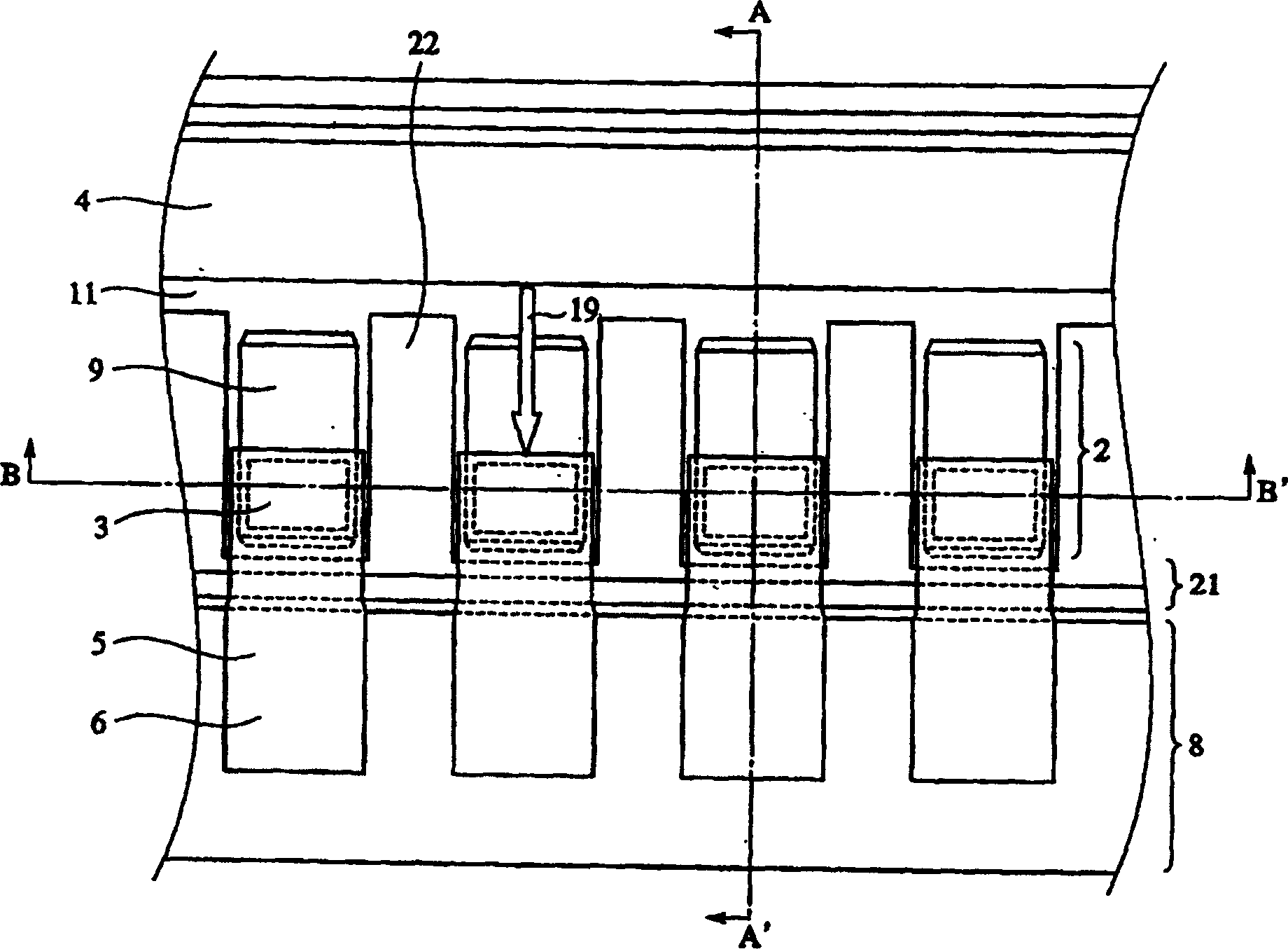
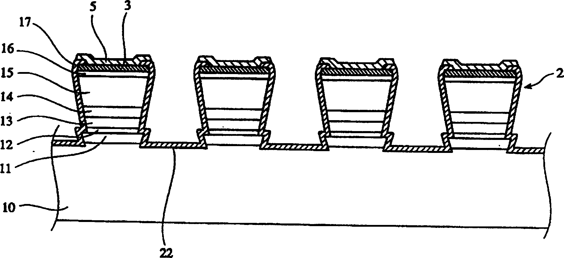
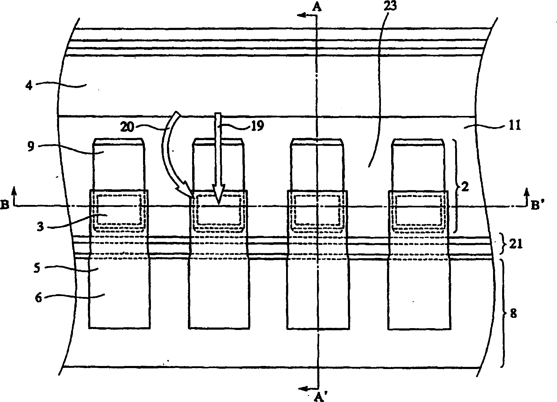
[0021] like figure 1 , figure 2 and Figure 4 ( figure 1 The A-A′ section and image 3 As shown in the A-A' cross-section of the same), the light emitting diode array of the present invention has a substrate 10, a conductive layer 11 formed on the entire surface of the substrate 10, a plurality of light emitting parts 2 independently formed on the conductive layer 11, and a plurality of light emitting parts 2 in the light emitting part 2. The first electrode 3 partially formed thereon and the second electrode 4 formed on the conductive layer 11 at a position close to the light emitting portion 2 . In addition, in figure 1 In , the insulating layer is omitted to clearly show the underlying layer. In the illustrated embodiment, each light-emitting portion 2 is provided with mesa-type etching grooves on the epitaxial layer uniformly formed on the substrate 10 , and is a part of each independent epitaxial layer portion.

[0022] (1) Su...


PUM


Abstract

The present invention relates to a light-emitting diode array for large light-emitting output, especially for a light-emitting diode array adapt for printer light source of the electronic photo manner. A light-emitting diode array comprising a conductive layer formed on a substrate, a plurality of separate light-emitting parts formed on the conductive layer, a first electrode formed on at least part of a top surface of each light-emitting part, and a second electrode formed on the conductive layer near the light-emitting part, the second electrode being a common electrode for operating a plurality of the light-emitting parts, and regions of the conductive layer between the adjacent light-emitting parts being removed.

Description

technical field [0001] The present invention relates to a light emitting diode array having a large luminous output, and in particular to a light emitting diode array applicable to a light source of an electrophotographic printer. Background technique [0002] Electrophotographic printers use light corresponding to image signals to form electrostatic latent images on photosensitive drums, selectively attach toners for development, and copy images on paper to obtain images. Laser methods and light-emitting diode array methods are widely used. As a light source for forming a latent image. In particular, the light source of the light-emitting diode array method does not need to take a long optical path like the laser method, so it is suitable for small printers or large-scale printing. In recent years, with the increase in printing speed and high image quality and the continuous miniaturization of printers, higher-definition and high-output light-emitting diode arrays are requ...

Claims


Application Information

Patent Timeline
Patent Type & Authority Patents(China)
IPC IPC(8): G03G15/04H01L33/00B41J2/45H01L27/15H01L33/08H01L33/14H01L33/30H01L33/40
CPCH01L27/153B41J2/45
Inventor 行本富久
Owner HITACHI CABLE
Why Eureka
Try Eureka