Light-emitting element array, and light exposure head and image forming apparatus using the same

Inactive Publication Date: 2019-06-06
CANON KK
View PDF5 Cites 0 Cited by
  • Summary
  • Abstract
  • Description
  • Claims
  • Application Information

AI Technical Summary

Benefits of technology

The present invention is about improving the reliability of a light exposure head and an image forming apparatus by increasing the light emitting output of each light emitting thyristor and reducing the variation in the light emitting output of each light emitting thyristor. This is achieved by forming a current constriction region in the light emitting thyristor and ensuring a minimum distance of at least 4 μm between the current constriction region and the side surface of the mesa structure. This configuration reduces light emitting loss and prevents sharp changes in light emitting output, resulting in a more reliable and effective light exposure head and image forming apparatus.

Problems solved by technology

It is said that, in a light emitting thyristor having a mesa structure, non-light-emitting recombination on a side surface of the mesa structure is one of the factors that reduce the light emitting efficiency.

Method used


Image

  • Light-emitting element array, and light exposure head and image forming apparatus using the same
  • Light-emitting element array, and light exposure head and image forming apparatus using the same
  • Light-emitting element array, and light exposure head and image forming apparatus using the same

Examples


first exemplary embodiment

[0024]According to a first exemplary embodiment of the present invention, a contact layer is formed on the fourth semiconductor layer in the semiconductor stacked structure of each thyristor and the current constriction region is defined by a region in which the contact layer is in contact with the fourth semiconductor layer.

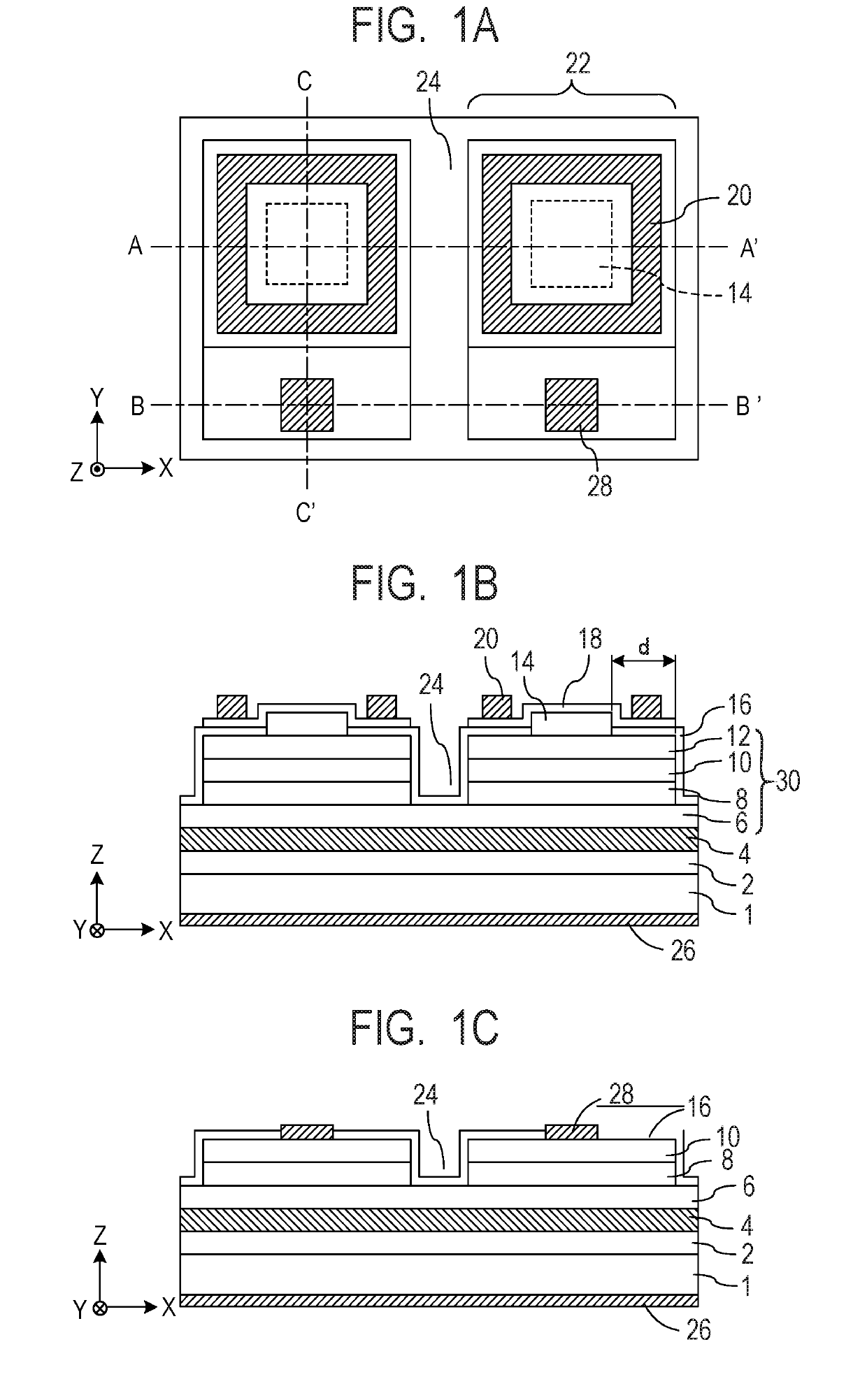
[0025]FIGS. 1A to 1C schematically illustrate the configuration according to the present exemplary embodiment, and also illustrate two light emitting thyristors. FIG. 1A is a plan view. FIG. 1B is an end view taken along a line A-A′ in FIG. 1A, and illustrates a sectional structure of an anode portion in each light emitting thyristor. FIG. 1C is an end view taken along a line B-B′ in FIG. 1A, and illustrates a sectional structure of a gate portion in each light emitting thyristor.

[0026]Each light emitting thyristor having the mesa structure includes an anode electrode and a gate electrode on the mesa structure. The anode electrode includes an opening. In the pre...

second exemplary embodiment

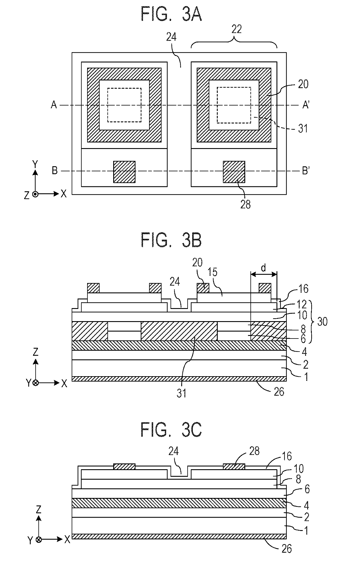
[0046]According to a second exemplary embodiment of the present invention, at least one of the semiconductor layers included in the semiconductor stacked structure of the thyristor 30 includes a first region and a second region having a resistance value higher than the resistance value of the first region within a plane viewed along the stacking direction, and the current constriction region is defined by the first region. Components other than the components described above are basically similar to those of the first exemplary embodiment. Accordingly, only the components different from those of the first exemplary embodiment will be described below.

[0047]FIGS. 3A to 3C schematically illustrate the configuration according to the present exemplary embodiment, and illustrate two light emitting thyristors 22. FIG. 3A is plan view, and FIG. 3B is an end view taken along the line A-A′ in FIG. 3A, and illustrates a sectional structure of an anode portion of each of the light emitting thyr...

examples

[0093]The light-emitting element array according to the first exemplary embodiment illustrated in FIGS. 1A to 1C was prepared, and the light emitting output at the side surface distance d and variations in light emission were examined.

[0094]On the n-type GaAs substrate 1, the buffer layer 2 made of n-type GaAs was epitaxially grown. Next, as the DBR layer 4, 20 pairs of n-type high-Al-composition AlGaAs and low-Al-composition AlGaAs were alternately stacked so that the optical length of each layer was set to ¼ of the light emitting wavelength λ of the light emitting thyristor 30. Next, n-type AlGaAs having an Al composition of 25% and an impurity concentration of 2×10¹⁸ / cm3 was stacked with a thickness of 600 nm as the cathode layer 6, and p-type AlGaAs having an Al composition of 15% and an impurity concentration of 3×10¹⁷ / cm3 was stacked with a thickness of 700 nm as the p-type gate layer 8. Next, n-type AlGaAs having an Al composition of 15% and an impurity concentration of 3×101...


PUM


Abstract

In a light-emitting element array using light emitting thyristors, a light emitting output of each light emitting thyristor can be increased and a variation in the light emitting output can be suppressed. On a substrate, a thyristor having a mesa structure including a cathode layer, a gate layer, a gate layer, and an anode layer is formed. A contact layer is formed on the anode layer. A current constriction region is formed by a region in which the anode layer is in contact with the contact layer. A minimum distance from the current constriction region to a side surface of the mesa structure is greater than or equal to 4 μm.

Description

BACKGROUND OF THE INVENTIONField of the Invention[0001]The present invention relates to a light-emitting element array used for a light exposure head of an electrophotographic printer.Description of the Related Art[0002]In electrophotographic printers, a method in which a photosensitive drum is exposed to light using a light exposure head and a latent image is formed is generally known. The light exposure head includes a light-emitting element array including an array of light-emitting elements disposed in a longitudinal direction of the photosensitive drum, and a rod lens array that focuses light from the light-emitting element array on the photosensitive drum. In this case, the length of the light-emitting element array is determined depending on the width of an image region on the photosensitive drum, and a pitch between light-emitting elements is determined depending on the resolution of the printer. For example, in the case of a printer with a resolution of 1200 dpi, the pitch ...

Claims


Application Information

Patent Timeline
IPC IPC(8): B41J2/45H01L27/15H01L33/00H01L33/10H01L33/14H01L33/20H01L33/30
CPCB41J2/45H01L27/153H01L33/0016H01L33/10H01L33/14H01L33/20H01L33/30H01L33/38
Inventor NAKANISHI, KOICHIROUCHIDA, TAKESHI
Owner CANON KK
Why Eureka
Try Eureka