Sense amplifier and semiconductor memory device having sense amplifier

a technology of sense amplifier and semiconductor memory device, which is applied in the direction of amplifiers with semiconductor devices/discharge tubes, dc-amplifiers with dc-coupled stages, instruments, etc., can solve the problems of limiting the reduction of the offset voltage of the sense amplifier, inability to achieve high-speed operation, and inability to meet the requirements of manufacturing conditions, etc., to achieve easy and effective reduction of offset voltage, reduce the variation of offset voltage, and reduce the effect of offset variation of offset variation

Active Publication Date: 2010-03-18
RENESAS ELECTRONICS CORP
View PDF0 Cites 22 Cited by
  • Summary
  • Abstract
  • Description
  • Claims
  • Application Information

AI Technical Summary

Benefits of technology

[0019]The systematic offset component is intentionally designed to be one polarity, while the offset voltage is switchable to the other polarity depending on the random offset component. More specifically, the capacitance load is switchable depending on the random offset component of each manufactured sense amplifier. After the sense amplifier is manufactured, the capacitance load is selec...

Problems solved by technology

Even in this case, however, the variation in device characteristics due to variation in a size of a fabricated gate electrode, variation in the number of ions injected, non-uniformity of manufacturing conditions and the like is inevitable in principle.
Thus, there is a limit to t...

Method used


Image

  • Sense amplifier and semiconductor memory device having sense amplifier
  • Sense amplifier and semiconductor memory device having sense amplifier
  • Sense amplifier and semiconductor memory device having sense amplifier

Examples


first embodiment

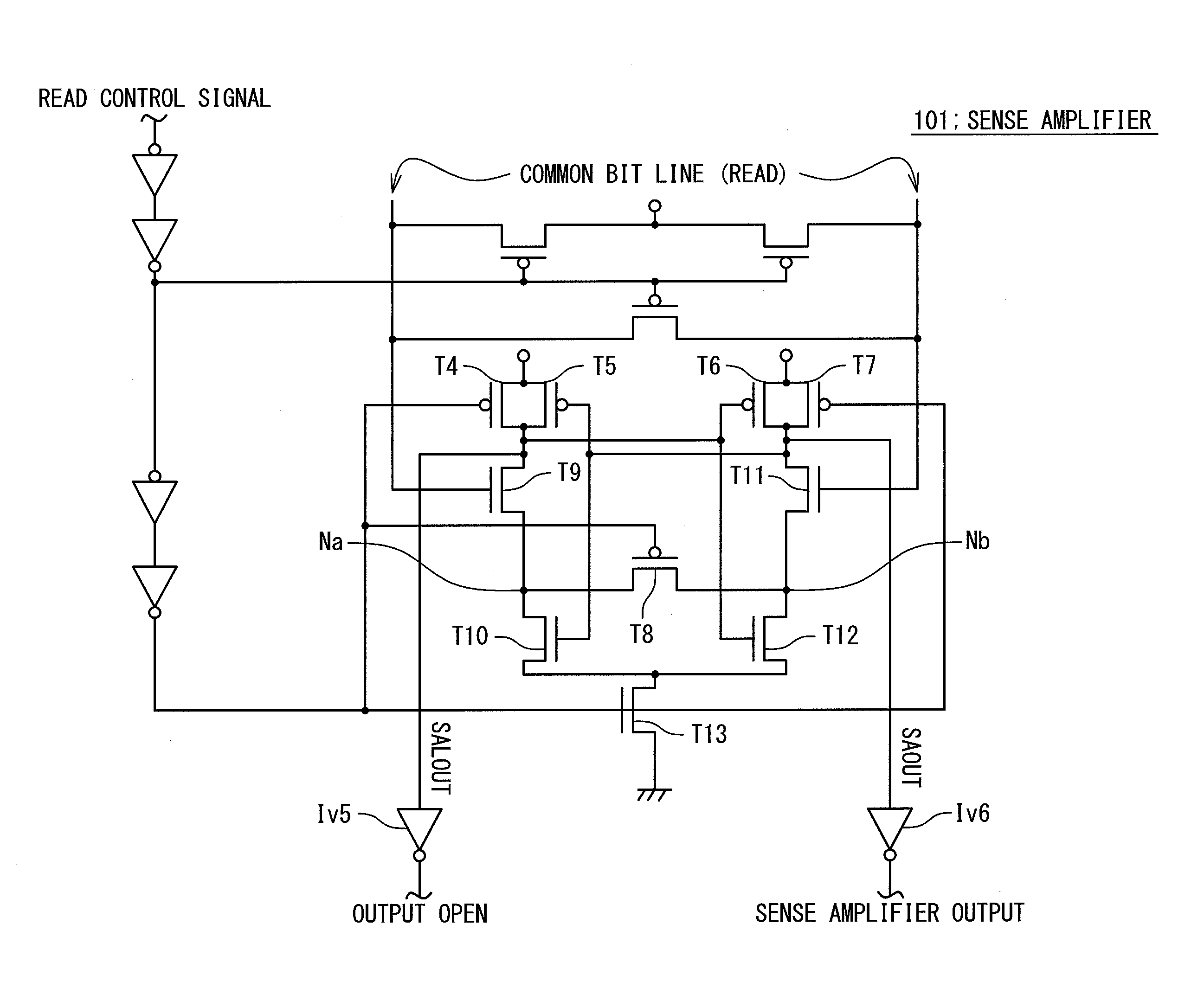
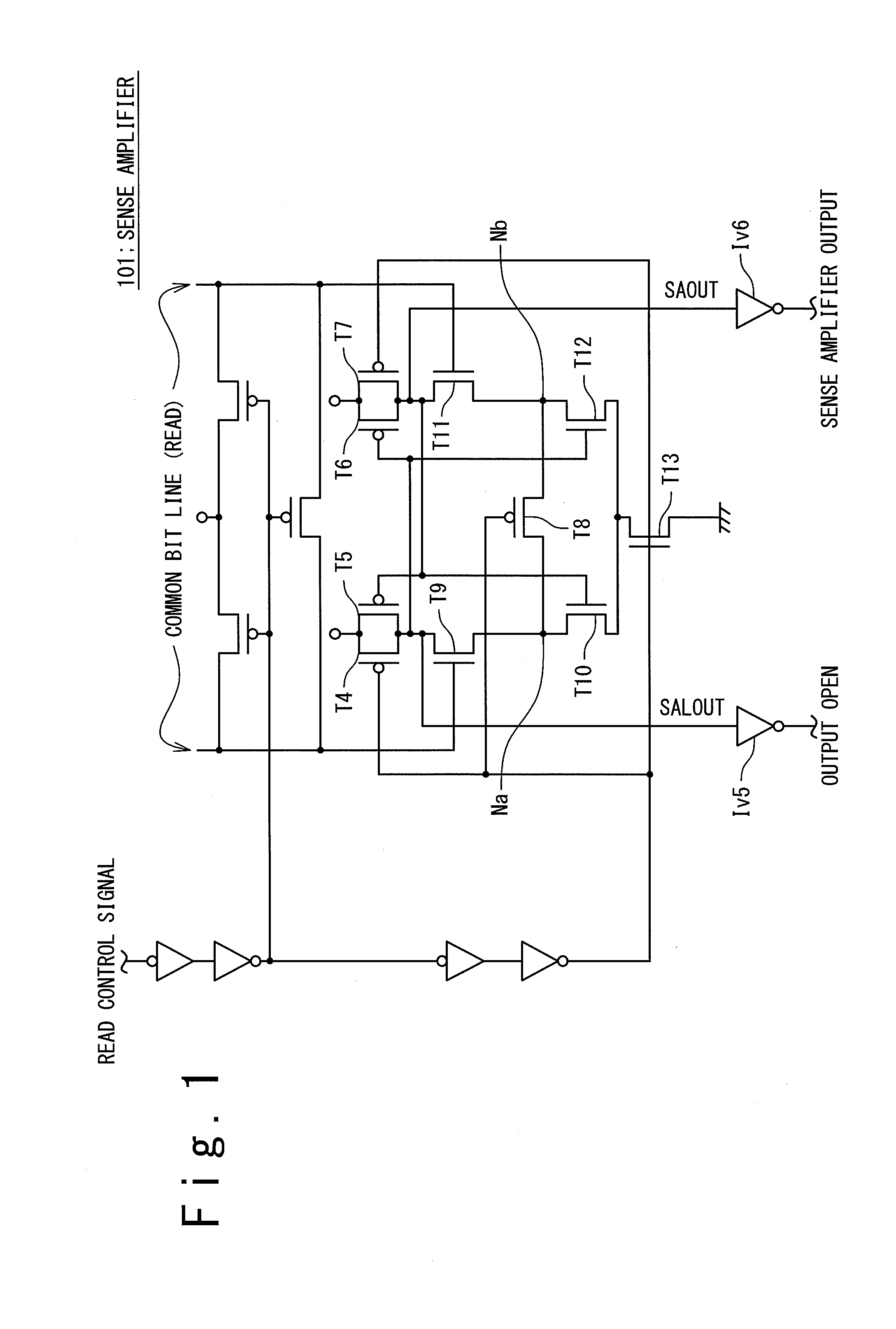
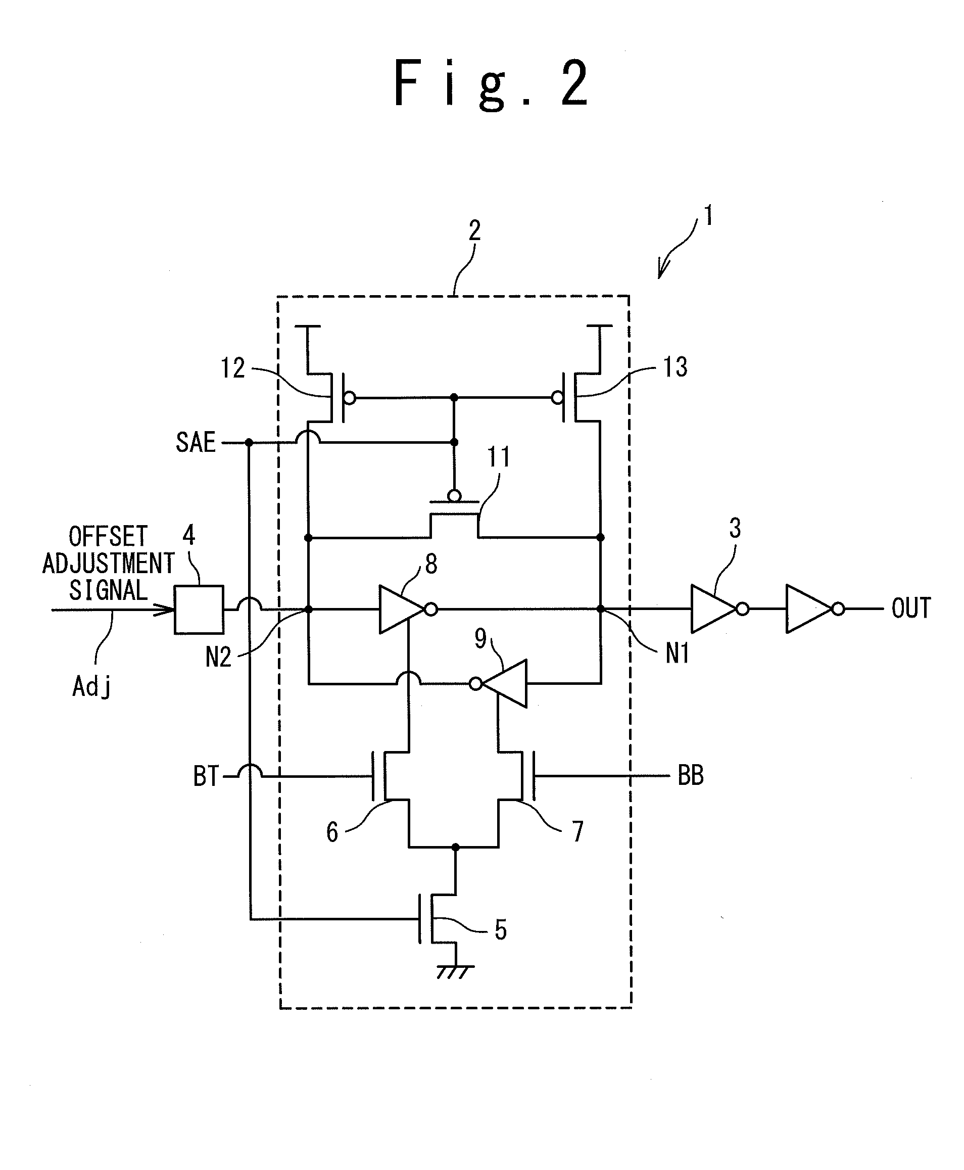
[0033]FIG. 2 is a circuit diagram showing a configuration example of a sense amplifier 1 according to a first embodiment of the present invention. The sense amplifier 1 is applied to a semiconductor memory device such as a DRAM and the like. The semiconductor memory device has a plurality of memory cells. The sense amplifier 1 amplifies a signal read out from at least one of the plurality of memory cells. More specifically, the sense amplifier 1 has a differential amplifier circuit 2, an output circuit 3 and a dummy load 4.

[0034]The differential amplifier circuit 2 has a switch transistor 5, a first differential transistor 6, a second differential transistor 7, a first inverter 8, a second inverter 9, a first PMOS transistor 11, a second PMOS transistor 12 and a third PMOS transistor 13. A sense amplifier enable signal SAE output from a read / write control circuit (not shown) is supplied to gates of the first to third PMOS transistors 11 to 13. The sense amplifier enable signal SAE i...

second embodiment

[0054]A second embodiment of the present invention will be described below. FIG. 10 is a circuit diagram showing a configuration example of a sense amplifier according to the second embodiment. The sense amplifier 1 in the second embodiment includes a control circuit 21. The control circuit 21 has functions of determining whether to set the offset adjustment signal Adj to “Disable” or “Enable”, retaining the determined offset adjustment signal Adj, and supplying the offset adjustment signal Adj to the dummy load 4.

[0055]As shown in FIG. 10, the control circuit 21 includes a NMOS transistor 22, a NMOS transistor 23, a capacitor 24, an inverter 25, an inverter 26, an offset set transistor 27 and an offset reset transistor 28. The capacitor 24 and the NMOS transistor 22 or the NMOS transistor 23 corresponds to and functions as the above-mentioned dummy load 4. The inverter 25 and the inverter 26 constitute a latch circuit to retain a data corresponding to the offset adjustment signal A...


PUM


Abstract

A sense amplifier comprises: a differential amplifier circuit configured to generate an amplified signal depending on a difference in voltage between bit lines; an output circuit receiving the amplified signal; and a load. The differential amplifier circuit comprises: a first output node supplying the amplified signal to the output circuit; and a second output node symmetrically placed with respect to the first output node and connected to the load. The output circuit comprises an output terminal for outputting an output signal generated based on the amplified signal. In response to a control signal, the load switches between a first capacitance value with which an offset voltage at the output terminal becomes a first voltage and a second capacitance value with which the offset voltage becomes a second voltage

Description

INCORPORATION BY REFERENCE[0001]This application is based upon and claims the benefit of priority from Japanese patent application No. 2008-238842, filed on Sep. 18, 2008, the disclosure of which is incorporated herein in its entirety by reference.BACKGROUND OF THE INVENTION[0002]1. Field of the Invention[0003]The present invention relates to a sense amplifier and a semiconductor memory device having the sense amplifier.[0004]2. Description of Related Art[0005]With improvement in a semiconductor technology, a semiconductor memory device in which increase in a chip area is suppressed and amount of memory is increased has been widely prevalent. A semiconductor memory device has a plurality of memory cells. Each memory cell stores one bit that is the minimum unit of information. For suppressing increase in the chip area and increasing the amount of memory, each memory cell has been miniaturized such that memory cells can be placed densely within a predetermined region.[0006]It's often ...

Claims


Application Information

Patent Timeline
IPC IPC(8): G11C7/02H03F3/45
CPCG11C7/065G11C2207/2254G11C11/4091G11C7/08
Inventor SENOU, TAKEFUMI
Owner RENESAS ELECTRONICS CORP
Why Eureka
Try Eureka