Manufacturing method of semiconductor device

a manufacturing method and semiconductor technology, applied in the field of semiconductor devices, can solve the problems of difficult to control the diameter of the silicon dot, increase of density, and difficulty in increasing the variation of the threshold voltage, and achieve the effects of high reliability of semiconductor devices, low cost, and increased density of silicon particles to serve as charge accumulating layers

Inactive Publication Date: 2008-02-26
SEMICON ENERGY LAB CO LTD
View PDF13 Cites 22 Cited by
  • Summary
  • Abstract
  • Description
  • Claims
  • Application Information

AI Technical Summary

Benefits of technology

[0008]The silicon dot is several nm long in diameter. Thus, the number of electrons injected into each dot is small by an influence of a quantum efficiency such as Coulomb blockade phenomenon, and the variation of a threshold voltage is also small. The density of silicon dots may be increased (i.e., the number of silicon dots per unit area may be increased) so that the variation of the threshold voltage can be large. However, because silicon dots are formed on the same plane, there is a limitation on the increase of the density and thus, it is difficult to increase the variation of the threshold voltage. Although the density may be increased by stacking silicon dots three-dimensionally, formations of an oxide film for isolating silicon dots and silicon dots are to be repeated to stack silicon dots three-dimensionally, thereby increasing the number of steps. Accordingly, there is a problem in that throughput is decreased and cost is increased.
[0012]According to the present invention, sputtering using, as a target, a solid solution containing a metal element and silicon that exceeds a solid solubility limit with respect to the metal element is conducted to form a conductive film, which has silicon particles and a layer containing the metal element, over an insulating film, and then the layer of the metal element is removed to expose the silicon particles. Thus, a semiconductor device having a memory transistor using the silicon particles as a floating gate electrode can be manufactured.
[0013]In addition, according to the present invention, sputtering using, as a target, a solid solution containing a metal element and silicon that exceeds a solid solubility limit with respect to the metal element is conducted to form a conductive film, which has silicon particles and a layer containing the metal element, over an insulating film, and then the layer of the first metal element is oxidized to form a metal oxide film. Thus, a semiconductor device having a memory transistor using the silicon particles as a floating gate electrode can be manufactured.
[0015]By a sputtering method, a semiconductor device having a floating gate electrode of silicon particles over a large substrate can be manufactured. Accordingly, because a semiconductor device can be manufactured by cutting out a plurality of thin film integrated circuits after a thin film circuit having a memory transistor is formed using a large substrate, a large number of semiconductor devices can be manufactured once and highly reliable semiconductor devices can be manufactured at low cost.
[0016]Since silicon particles dispersed three dimensionally can be formed by a sputtering method, the density of silicon particles to serve as a charge accumulating layer can be increased. The size of a silicon particle can be increased preventing a large number of silicon particles from being unified; therefore the amount of charges injected into each particle and the variation of a threshold voltage can be increased.
[0017]In a memory transistor, a threshold voltage of the memory transistor is increased when electrons are injected into a floating gate electrode. The memory transistor has information about either 0 or 1 depending on the threshold voltage. Accordingly, a nonvolatile memory in which a margin for reading electrically can be kept wide and data breakage is difficult to be caused can be manufactured by increasing the variation of the threshold voltage.

Problems solved by technology

Accordingly, there is a problem in that it is difficult to control the diameter of the silicon dot.
However, because silicon dots are formed on the same plane, there is a limitation on the increase of the density and thus, it is difficult to increase the variation of the threshold voltage.
Accordingly, there is a problem in that throughput is decreased and cost is increased.
Consequently, a highly reliable semiconductor nonvolatile memory element cannot be manufactured, because it has the same structure as a conventional semiconductor nonvolatile memory element in which a conductive layer or a polysilicon layer is a floating gate electrode.

Method used


Image

  • Manufacturing method of semiconductor device
  • Manufacturing method of semiconductor device
  • Manufacturing method of semiconductor device

Examples


embodiment mode 1

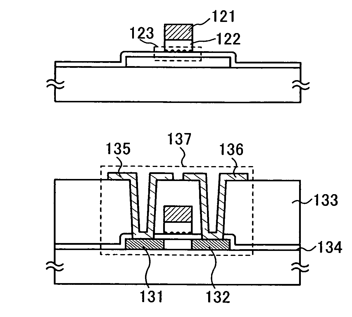
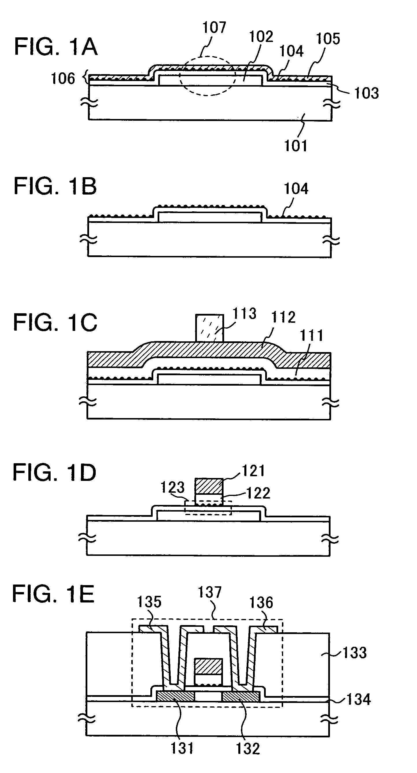
[0040]Embodiment Mode 1 describes a manufacturing process of a nonvolatile memory having silicon dots with reference to FIGS. 1A to 1E.

[0041]As shown in FIG. 1A, a semiconductor region 102 is formed over a substrate 101. Then, a first insulating film 103 is formed over the substrate and the semiconductor region. A first conductive layer 106 is formed over the first insulating film 103. The first conductive layer 106 includes silicon particles 104 and a conductive layer 105.

[0042]As the substrate 101, a glass substrate, a quartz substrate, a ceramic substrate, a plastic substrate, a stainless substrate, a synthetic resin substrate, a flexible substrate, a single crystal semiconductor substrate (typically, an n-type or p-type single crystal silicon substrate, GaAs substrate, InP substrate, GaN substrate, SiC substrate, or ZnSe substrate) and the like can be nominated. An SOI (Silicon on Insulator) substrate may also be used. In the case of using any one of these substrates, a base fil...

embodiment mode 2

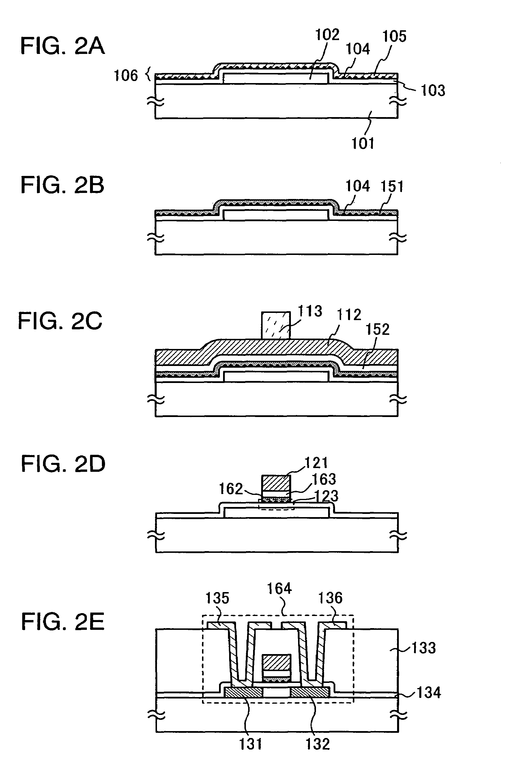
[0084]Embodiment Mode 2 describes a manufacturing method of a memory transistor in which an insulating film is formed by oxidizing a conductive layer over silicon particles as in Embodiment Mode 1 with reference to FIGS. 2A to 2E.

[0085]As shown in FIG. 2A, a semiconductor region 102 and a first insulating film 103 are formed over a substrate 101 according to Embodiment Mode 1. Then, a first conductive film 106 containing silicon particles 104 and a conductive layer 105 is formed over the first insulating film 103 by a sputtering method. Here, a solid solution containing silicon that exceeds solid solubility limit with respect to a metal element is used as a target in the sputtering. As the metal element that can form a solid solution with silicon, metal elements such as berylium (Be), aluminum (Al), zinc (Zn), gallium (Ga), germanium (Ge), silver (Ag), cadmium (Cd), indium (In), tin (Sn), antimony (Sb), lead (Pb) and bismuth (Bi), which are solid-dissolved with silicon and are easil...

embodiment mode 3

[0097]Embodiment Mode 3 describes a manufacturing process of a memory transistor formed with different masks for a gate electrode and a floating gate electrode with reference to FIGS. 3A to 3E.

[0098]As shown in FIG. 3A, a semiconductor region 102 and a first insulating film 103 are formed over a substrate 101 according to Embodiment Mode 1. Then, a first conductive film 106 containing silicon particles 104 and a conductive layer 105 is formed over the first insulating film 103 by a sputtering method. As shown in FIG. 3B, the conductive layer 105 is removed as in Embodiment Mode 1 to expose silicon particles. A first mask pattern 171 is formed over the silicon particles 104 and the first insulating film 103. The first mask pattern 171 is a mask pattern for forming a floating gate electrode later.

[0099]The silicon particles are etched using the first mask pattern 171 to form a floating gate electrode 172 of silicon particles as shown in FIG. 3C. A second insulating film 111 and a seco...


PUM


Abstract

The present invention provides a manufacturing method of a semiconductor device having a semiconductor nonvolatile memory element that is highly reliable and that can increase a variation of a threshold voltage. Further, the present invention provides a method for manufacturing a semiconductor device having a highly reliable semiconductor nonvolatile memory element using a large substrate. According to the present invention, sputtering using, as a target, a solid solution containing silicon that exceeds a solid solubility limit is conducted, so that a conductive film including a conductive layer of a metal element that is a main component of the solid solution and silicon particles is formed, and then, the conductive layer of the metal element is removed to expose silicon particles. Furthermore, a semiconductor device having a semiconductor nonvolatile memory element using the silicon particles as a floating gate electrode is manufactured.

Description

BACKGROUND OF THE INVENTION[0001]1. Field of the Invention[0002]The present invention relates to a semiconductor device having a semiconductor nonvolatile memory element, specifically, relates to a method for manufacturing of a semiconductor device including a floating gate electrode formed with semiconductor particles.[0003]2. Description of the Related Art[0004]EEPROM (Electrically Erasable and Programmable Read Only Memory) and a flash memory are know n as a memory representing a semiconductor nonvolatile memory. As for the nonvolatile memory, a conductive layer serving as a charge accumulating layer or a floating gate type memory including a polysilicon layer is representative.[0005]With recent reduction of devices in size, thinning of a tunnel oxide film of a semiconductor nonvolatile memory has been conducted. In the current situation, there is caused a defect such as a deterioration of the tunnel oxide film caused in forming films or a set of operation such as writing or eras...

Claims


Application Information

Patent Timeline
Patent Type & Authority Patents(United States)
IPC IPC(8): H01L21/8247G11C16/04G11C16/06H01L21/28H01L21/336H01L29/423H01L29/788
CPCB82Y10/00G11C16/04H01L21/28273H01L24/32H01L29/42332H01L29/66825H01L29/7881G11C2216/06H01L2224/32225H01L2224/48091H01L2224/48227H01L2224/48465H01L2224/73265H01L2924/01004H01L2924/01013H01L2924/01029H01L2924/0103H01L2924/01032H01L2924/01046H01L2924/01047H01L2924/01049H01L2924/0105H01L2924/01051H01L2924/0106H01L2924/01073H01L2924/01077H01L2924/01078H01L2924/01079H01L2924/01082H01L2924/15184H01L2924/15311H01L2924/19041H01L2224/83385H01L2924/01005H01L2924/01006H01L2924/01019H01L2924/01023H01L2924/01024H01L2924/01033H01L2924/0104H01L2924/01041H01L2924/01042H01L2924/01045H01L2924/01072H01L2924/01074H01L2924/10329H01L2924/0132H01L2924/07811H01L2924/13091H01L2924/00014H01L2924/00H01L2924/01014H01L2924/00012H01L2924/15787H01L2924/181H01L2924/12042H01L24/73H01L2924/14H01L29/40114
Inventor YAMAGUCHI, TETSUJITOKUNAGA, HAJIME
Owner SEMICON ENERGY LAB CO LTD
Why Eureka
Try Eureka