

Manufacturing method of substrate having conductive layer and manufacturing method of semiconductor device
a manufacturing method and technology of a semiconductor device, applied in the direction of semiconductor/solid-state device details, diodes, inductances, etc., can solve the problems of reducing yield, forming short circuits of conductive layers, and reducing yield, so as to achieve uniform width and distance of conductive layers, and uniform thickness of conductive layers
- Summary
- Abstract
- Description
- Claims
- Application Information
AI Technical Summary
Benefits of technology
Problems solved by technology
Method used
Image

Examples
embodiment mode 1
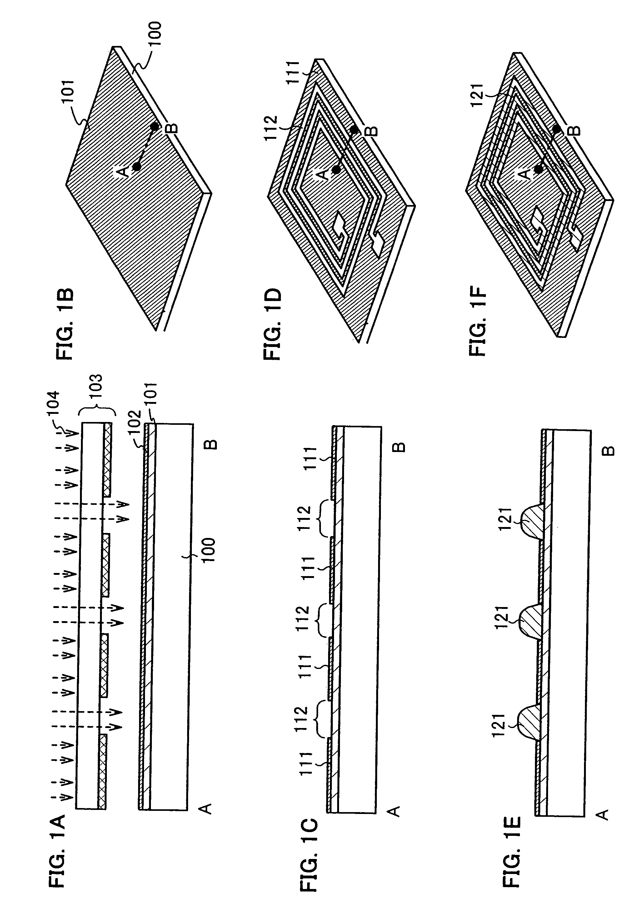
[0042]In this embodiment mode, steps of forming regions with different wettability over a substrate using a photomask, and steps of forming a conductive layer in the high wettability region are described with reference to FIGS. 1A to 1F. In this embodiment mode, description is made using an antenna as a typical example of a conductive layer.
[0043]FIGS. 1B, 1D and 1F are perspective views of a substrate having an antenna, and FIGS. 1A, 1C and 1E are cross sectional views along a line A-B.
[0044]An inorganic insulating layer 101 is formed over a substrate 100, and a low wettability layer 102 is formed over the inorganic insulating layer 101 (see FIGS. 1A and 1B).
[0045]The substrate 100 may be a glass substrate, a quartz substrate, a substrate made of an insulating substance such as ceramic such as alumina, a plastic substrate, a silicon wafer, a metal plate or the like.
[0046]The plastic substrate is typically made of polyethylene naphthalate (PEN), polypropylene, polypropylene sulfide,...
embodiment mode 2
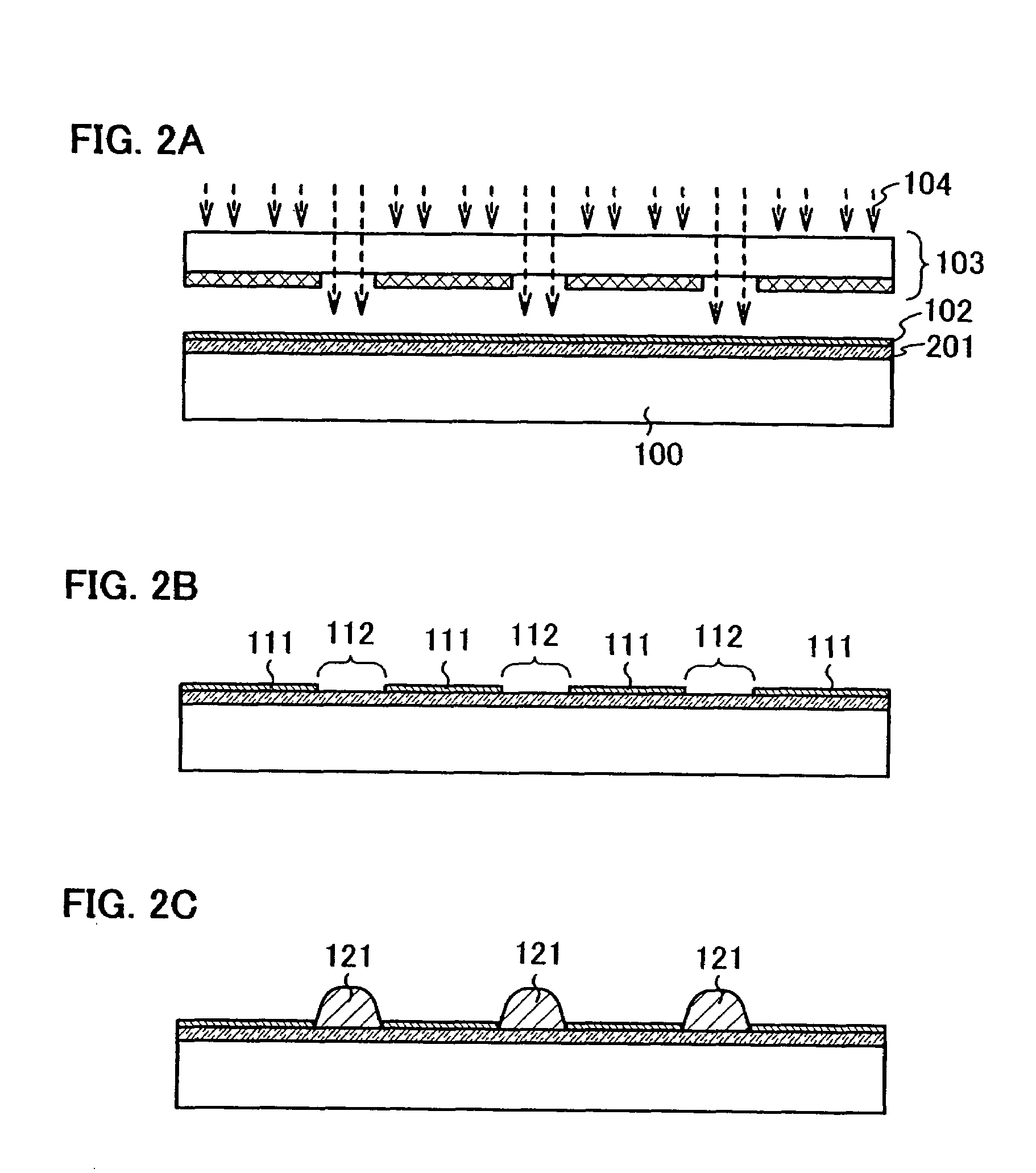
[0073]In this embodiment mode, manufacturing steps of a conductive layer forming region, which are effectively performed compared to Embodiment Mode 1, are described with reference to FIGS. 2A to 2C. In this embodiment mode, a low wettability layer is effectively exposed to light using a photocatalytic layer.
[0074]A photocatalytic layer 201 is formed over the substrate 100, and the low wettability layer 102 is formed over the photocatalytic layer 201 (see FIG. 2A).
[0075]The photocatalytic layer 201 is formed of titanium oxide (TiOx), titanate (MTiO3) such as strontium titanate (SrTiO3), tantalate (MTaO3), niobate (M4Nb6O17), (note that every “M” indicates a metal element), cadmium sulfide (Cds), zinc sulfide (ZnS), cadmium selenide (CdSe), potassium tantalate (KTaO3), zirconium oxide (ZrO2), niobium oxide (Nb2O5), zinc oxide (ZnO), iron oxide (Fe2O3), tungsten oxide (WO3), or the like.
[0076]The photocatalytic layer 201 is formed by sputtering, plasma CVD, vapor deposition, sol-gel m...
embodiment mode 3
[0083]In this embodiment mode, a low wettability layer is exposed to light without using a photomask.
[0084]The inorganic insulating layer 101 is formed over the substrate 100, and photocatalytic layers 301 each having a desired shape are formed over the inorganic insulating layer 101 (see FIG. 3A). Then, a low wettability layer 302 is formed over the photocatalytic layers 301 and the inorganic insulating layer 101 (see FIG. 3B). In this embodiment mode, the photocatalytic layers 301 have the same shape as conductive layers that are formed later.
[0085]The photocatalytic layers 301 are irradiated with the light 104 to be activated. As a result, the low wettability layer 302 that is in contact with the photocatalytic layers 301 is selectively reacted, and the substance of the low wettability layer is decomposed, thereby forming high wettability regions 304. In this embodiment mode, the photocatalytic layers 301 are exposed in the high wettability regions 304; however, the invention is ...
PUM
| Property | Measurement | Unit |
|---|---|---|
| temperature | aaaaa | aaaaa |
| contact angle | aaaaa | aaaaa |
| contact angle | aaaaa | aaaaa |
Abstract
Description
Claims
Application Information