Light-emitting diode, light-emitting diode lamp, and illumination device

a technology of light-emitting diodes and diodes, which is applied in the direction of basic electric elements, electrical equipment, semiconductor devices, etc., can solve the problems of deterioration in light extraction efficiency and light absorption at the surface electrode pad portion, and achieve low forward voltage, reduced light absorption at the surface electrode, and high light emission output

Inactive Publication Date: 2017-07-11
SHOWA DENKO KK
View PDF19 Cites 0 Cited by
  • Summary
  • Abstract
  • Description
  • Claims
  • Application Information

AI Technical Summary

Benefits of technology

[0015]The present invention has been developed in light of the above circumstances, and has an object of providing a light-emitting diode, a light-emitting diode lamp and an illumination device in which light absorption at the surface electrode is reduced, and a low forward voltage is achieved, while maintaining a high light emission output, by improving the positional relationship of the ohmic electrodes that sandwich the compound semiconductor layer.
[0016]In order to achieve the above object, from the viewpoint of eliminating factors causing the absorption of the emitted light, a configuration was adopted in which the growth substrate was removed and replaced with a support substrate exhibiting less light absorption. Further, in this regard, in order to reduce the light absorption at the pad (bonding pad) portion of the surface electrode, a configuration was adopted in which no light emission was generated directly beneath the surface electrode pad portion. Furthermore, the inventors discovered that in a configuration in which, among the plurality of ohmic contact electrodes dispersed across the semiconductor substrate side of the compound semiconductor layer containing the light-emitting layer, a prescribed proportion of the ohmic contact electrodes are arranged in positions which, when viewed in plan view, overlap with linear portions of the surface electrode that are connected to the pad portion, a low forward voltage could be achieved while maintaining a high light emission output, and they were therefore able to complete the present invention. Conventionally, it had been thought that employing a configuration in which the plurality of ohmic contact electrodes dispersed across the semiconductor substrate side of the compound semiconductor layer containing the light-emitting layer were arranged in positions which, when viewed in plan view, did not overlap with the linear portions of the surface electrode that were connected to the pad portion enabled the current to disperse across the entire device, and was therefore preferable.
[0031]According to the light-emitting diode of the present invention, light absorption at the surface electrode is reduced, and a low forward voltage can be achieved while maintaining a high light emission output.

Problems solved by technology

However, a problem arises in that the bonding pad absorbs the light emitted by the light-emitting unit, causing a deterioration in the light extraction efficiency.
This problem of light absorption at the surface electrode pad portion is particularly marked in high-brightness light-emitting diodes.

Method used


Image

  • Light-emitting diode, light-emitting diode lamp, and illumination device
  • Light-emitting diode, light-emitting diode lamp, and illumination device
  • Light-emitting diode, light-emitting diode lamp, and illumination device

Examples


first embodiment

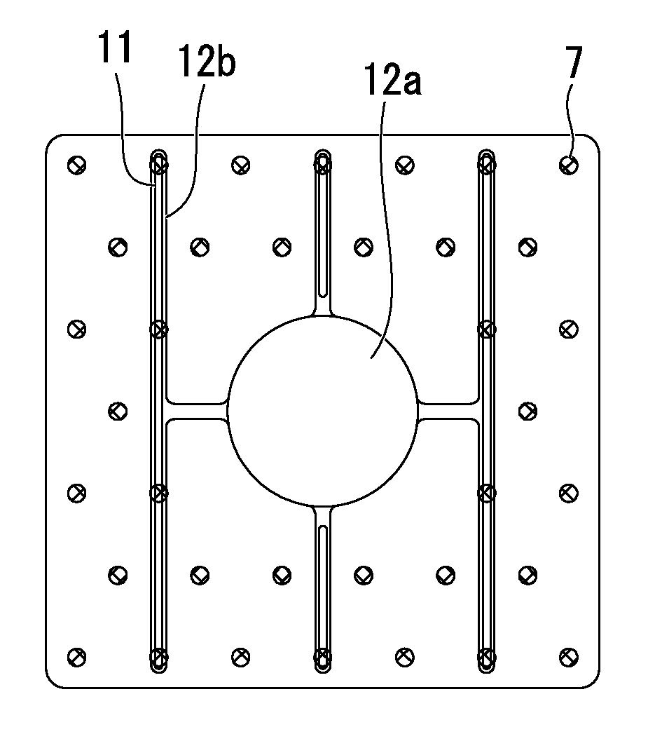
[0053][Light-Emitting Diode (First Embodiment)]

[0054]FIG. 1 is a schematic cross-sectional view illustrating one example of a light-emitting diode of an embodiment applicable to the present invention.

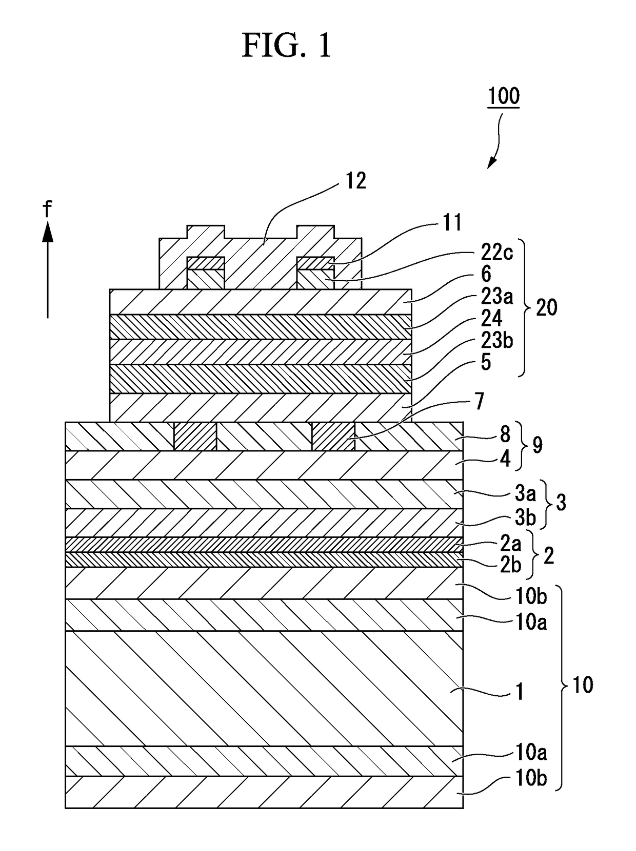
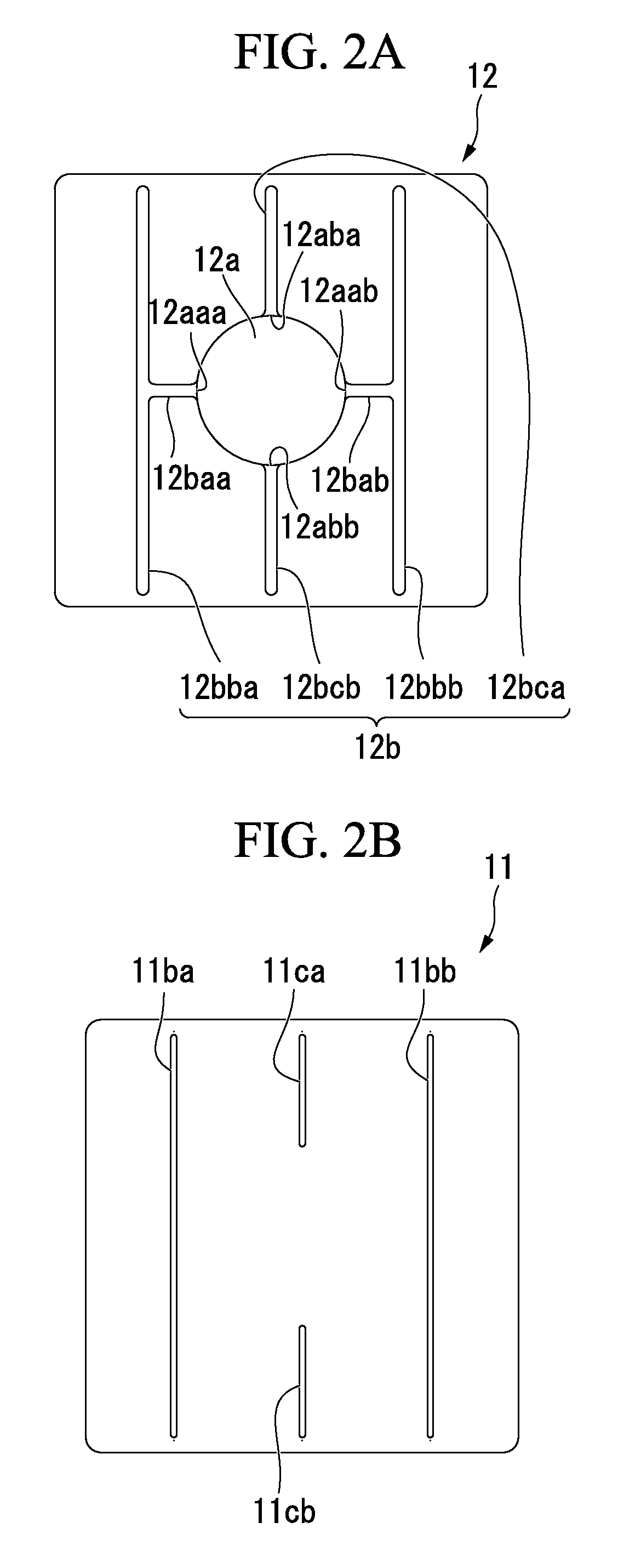
[0055]The light-emitting diode 100 of this embodiment includes a junction layer 2, a reflective structure 9 containing a metal reflective film 4, and a compound semiconductor layer 20 containing a light-emitting layer sandwiched between a first cladding layer and a second cladding layer, provided in that order on a semiconductor substrate 1, wherein a plurality of dot-shaped ohmic contact electrodes 7 are provided between the metal reflective film 4 and the compound semiconductor layer 20, an ohmic electrode 11 and a surface electrode 12 composed of a pad portion 12a (see FIG. 2A to 2D) and a plurality of linear portions 12b (see FIG. 2A to 2D) connected to the pad portion are provided in that order on the opposite side of the compound semiconductor layer from the semiconductor substrat...


PUM


Abstract

In a light-emitting diode, a plurality of dot-shaped ohmic contact electrodes are provided between a metal reflective film and a compound semiconductor layer, an ohmic electrode and a surface electrode composed of a pad portion and a plurality of linear portions connected to the pad portion are provided in that order on the opposite side of the compound semiconductor layer from the semiconductor substrate, the surface of the ohmic electrode is covered with the linear portions, the ohmic contact electrodes and the ohmic electrode are formed in positions that do not overlap with the pad portion in plan view, and among the plurality of ohmic contact electrodes, 5% or more and 40% or less of the ohmic contact electrodes are disposed in positions that overlap with the linear portions in plan view.

Description

CROSS REFERENCE TO RELATED APPLICATIONS[0001]This application is a National Stage of International Application No. PCT / JP2013 / 077334 filed Oct. 8, 2013, claiming priority based on Japanese Patent Application No. 2012-229183, filed Oct. 16, 2012, the contents of all of which are incorporated herein by reference in their entirety.BACKGROUND OF THE INVENTION[0002]Field of the Invention[0003]The present invention relates to a light-emitting diode, a light-emitting diode lamp and an illumination device, and relates particularly to a light-emitting diode, a light-emitting diode lamp and an illumination device which are suited to high-brightness light emission.[0004]Description of Related Art[0005]Examples of known high-brightness light-emitting diodes (English abbreviation: LED) which emit red or infrared light include compound semiconductor light-emitting diodes having a light-emitting layer formed from aluminum gallium arsenide (composition formula: AlXGa1−XAs, 0≦X≦1) or a light-emittin...

Claims


Application Information

Patent Timeline
Patent Type & Authority Patents(United States)
IPC IPC(8): H01L33/40H01L33/10H01L33/44H01L33/38H01L33/30H01L33/00
CPCH01L33/387H01L33/10H01L33/30H01L33/44H01L33/0079H01L33/405H01L33/0093
Inventor MATSUMURA, ATSUSHITOKUNAGA, YU
Owner SHOWA DENKO KK
Why Eureka
Try Eureka