Light-emitting diode and method for manufacturing tunnel junction layer

a technology of light-emitting diodes and manufacturing methods, which is applied in the direction of basic electric elements, electrical apparatus, semiconductor devices, etc., can solve the problems of reducing the light-emitting diodes' light emission output, and achieve the effect of improving light emission outpu

Active Publication Date: 2019-10-08
RESONAC PHOTONICS CORP
View PDF20 Cites 0 Cited by
  • Summary
  • Abstract
  • Description
  • Claims
  • Application Information

AI Technical Summary

Benefits of technology

The invention improves the output of a light-emitting diode that has multiple layers of light-emitting parts that are stacked one on top of each other. This is done by using a tunnel junction part.

Problems solved by technology

However, adopting this configuration may reduce light emission output of the light-emitting diode because, in some cases, a part of the light emitted from each light-emitting part cannot be extracted to the outside of the light-emitting diode.

Method used


Image

  • Light-emitting diode and method for manufacturing tunnel junction layer
  • Light-emitting diode and method for manufacturing tunnel junction layer
  • Light-emitting diode and method for manufacturing tunnel junction layer

Examples


examples

[0165]Hereinafter, the present invention will be described in more detail based on the Examples. However, it should be noted that the present invention is not limited to the Examples below as long as the gist of the present invention is maintained.

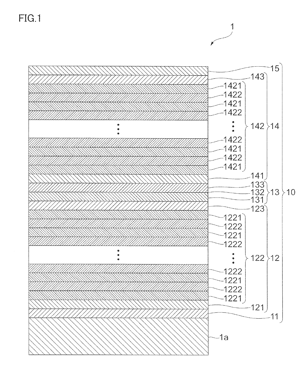
[0166]The inventors manufactured semiconductor layer forming substrates 1 each having a tunnel junction layer 13 of a different composition. The inventors then evaluated various properties of semiconductor light-emitting elements 2 obtained from the respective semiconductor layer forming substrates 1.

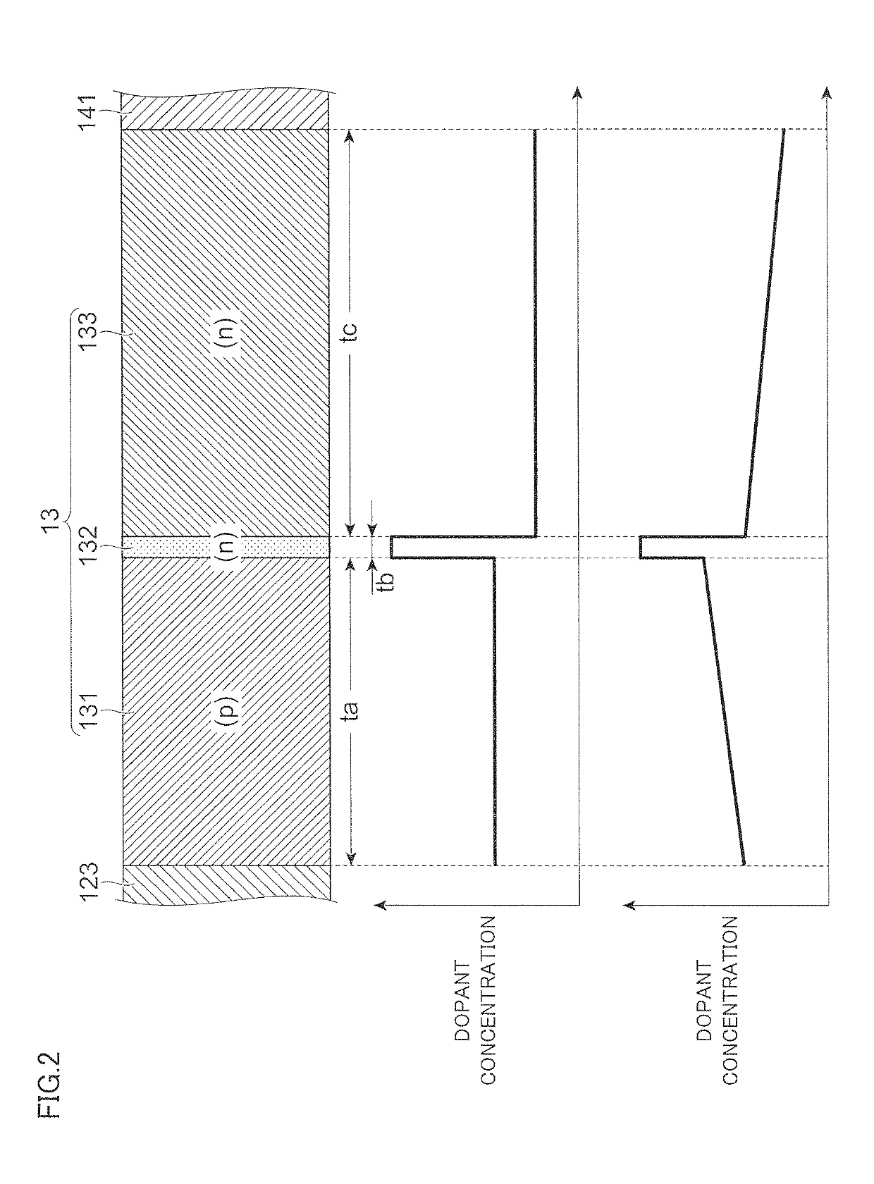
[0167]Table 1 shows conditions for manufacturing the semiconductor layer forming substrate 1 of the Example 1. Table 2 shows relationship between the tunnel junction layers of the semiconductor layer forming substrates 1 of the Examples 1 to 3 and the Comparative Example.

[0168]

TABLE 1 [EXAMPLE 1]EMISSION WAVELENGTH810 nmCONCEN-DOP-TRATIONTHICKNESSLAYER STRUCTUREMATERIALANT( / cm3)(μm)LIGHTP-TYPE CONTACT LAYER 15AlGaAsC3.0E+183.50EMITTINGSECOND L...


PUM


Abstract

A light-emitting element layer 10 includes: an n-type contact layer 11; a first light-emitting layer 12; a tunnel junction layer 13; a second light-emitting layer 14; and a p-type contact layer 15 laminated in this order. The first light-emitting layer 12 and the second light-emitting layer 14 emit light of the same wavelength. The tunnel junction layer 13 includes: a p-type tunnel layer 131 made of AlGaAs containing p-type impurities (C); and an n-type tunnel layer 133 made of GaInP containing n-type impurities (Te). A highly n-type impurities-doped layer 132 having a higher concentration of n-type impurities than the n-type tunnel layer 133 is arranged between the p-type tunnel layer 131 and the n-type tunnel layer 133.

Description

CROSS REFERENCE TO RELATED APPLICATIONS[0001]This application is based on and claims priority under 35 USC § 119 from Japanese Patent Application No. 2017-103197 filed May 25, 2017 and Japanese Patent Application No. 2018-017456 filed Feb. 2, 2018.BACKGROUNDTechnical Field[0002]The present invention relates to a light-emitting diode and a method for manufacturing a tunnel junction layer.Related Art[0003]A light-emitting diode has been widely known that includes a p-type semiconductor layer containing p-type impurities, an n-type semiconductor layer containing n-type impurities, and an active layer sandwiched between the p-type semiconductor layer and the n-type semiconductor layer and having a smaller band gap than the p-type semiconductor layer and the n-type semiconductor layer.[0004]Japanese Patent Application Laid-Open Publication No. 2009-522755 discloses a light-emitting diode that includes a first radiation-generating active layer and a second radiation-generating active laye...

Claims


Application Information

Patent Timeline
Patent Type & Authority Patents(United States)
IPC IPC(8): H01L33/06H01L33/00H01L33/30H01L33/40H01L33/04H01L33/08
CPCH01L33/0062H01L33/30H01L33/06H01L33/405H01L33/08H01L33/04H01L33/305
Inventor UZAWA, AKIRASEO, NORIYOSHIMATSUMURA, ATSUSHIAIHARA, NORIYUKI
Owner RESONAC PHOTONICS CORP
Why Eureka
Try Eureka