Semiconductor light emitting element and light emitting device

a technology of light emitting elements and semiconductors, applied in the direction of semiconductor/solid-state device manufacturing, semiconductor devices, electrical devices, etc., can solve the problems of reducing light emission output and reducing internal quantum efficiency, and achieve the effect of improving light emission outpu

Active Publication Date: 2015-02-24
TOYODA GOSEI CO LTD
View PDF16 Cites 0 Cited by
  • Summary
  • Abstract
  • Description
  • Claims
  • Application Information

AI Technical Summary

Benefits of technology

[0015]According to the present invention, it is possible to improve light emission output in the semiconductor light emitting element that emits light of the wavelength indicating green color by use of the group III nitride semiconductor.

Problems solved by technology

However, in the semiconductor light emitting element using the group III nitride semiconductor, in a case of employing a configuration that emits light of the wavelength indicating green color, large deformation is apt to occur in the light emitting layer and internal quantum efficiency tends to be reduced, to thereby reduce light emission output compared to a case of employing a configuration that emits light of blue color or ultraviolet light.

Method used


Image

  • Semiconductor light emitting element and light emitting device
  • Semiconductor light emitting element and light emitting device
  • Semiconductor light emitting element and light emitting device

Examples


examples

[0094]Hereinafter, the present invention will be described further in detail with reference to examples. However, the present invention is not limited to the following examples as long as the scope of the gist thereof is not exceeded.

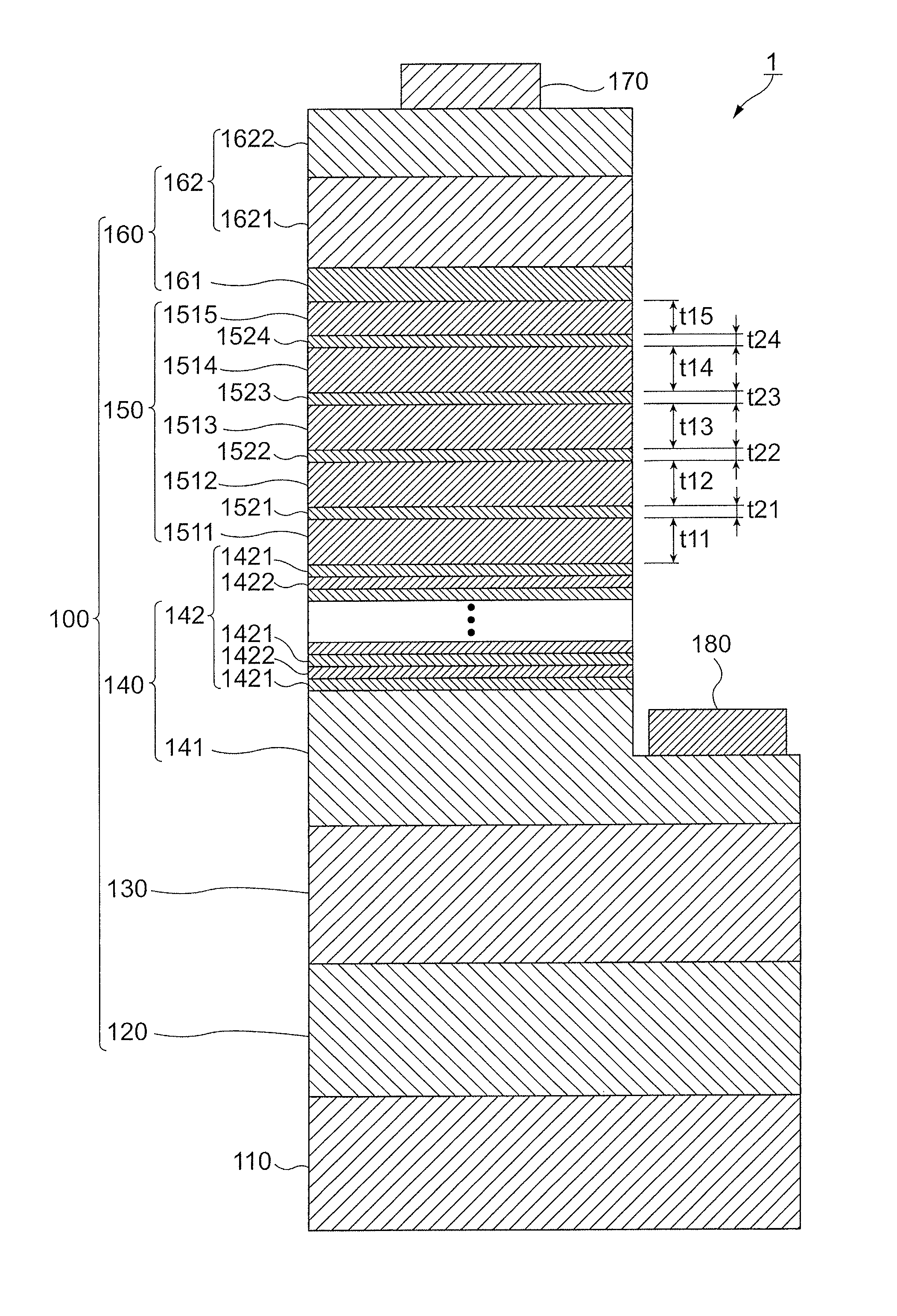
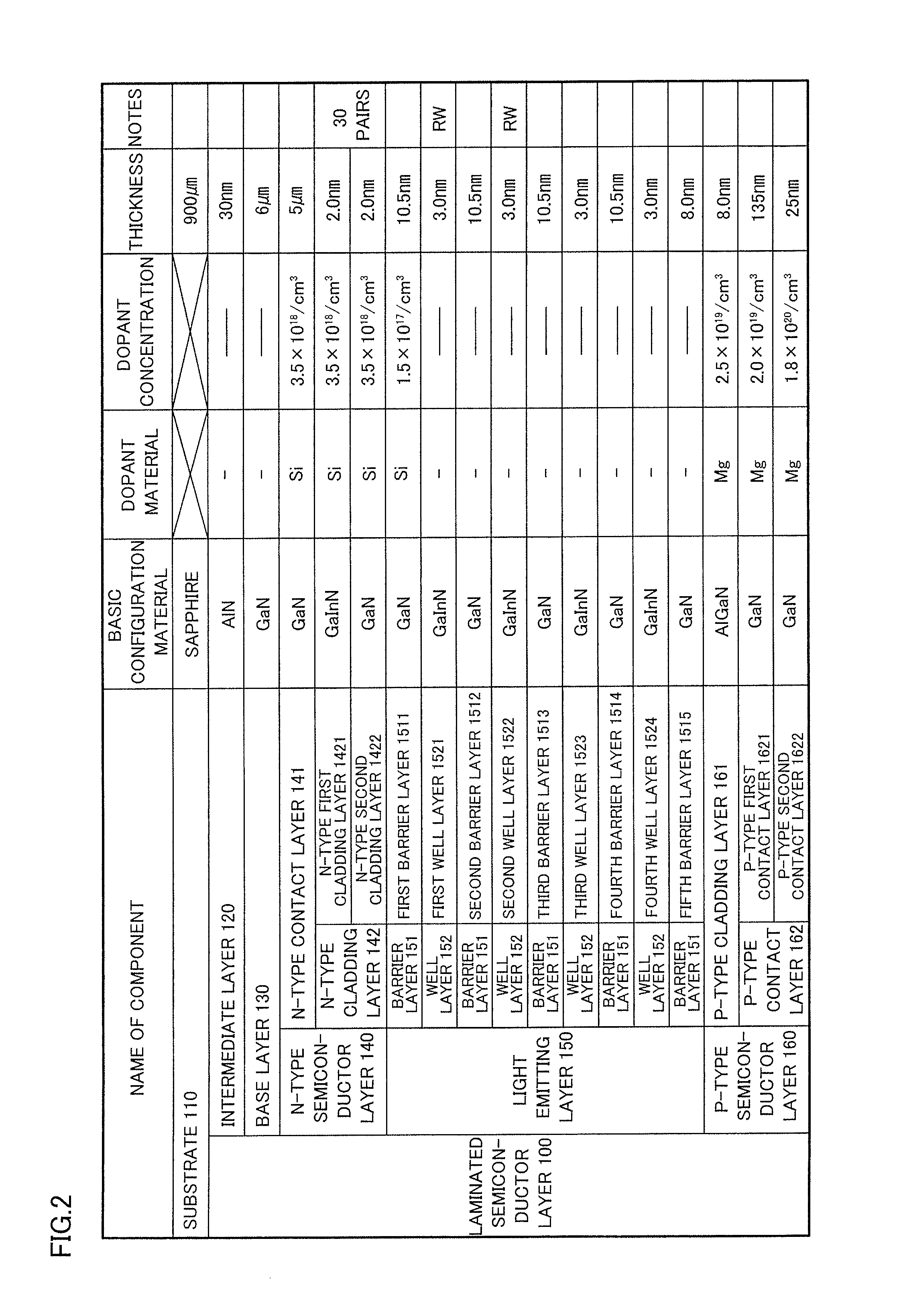
[0095]The present inventors formed the semiconductor light emitting elements 1 in which relationship between the compositions, structures and thicknesses are made variously different with respect to the barrier layer 151 (the first barrier layer 1511 to the fifth barrier layer 1515) and the well layer 152 (the first well layer 1521 to the fourth well layer 1524) in the light emitting layer 150, and performed evaluations related to the light emission output.

[0096]Here, Table 1 shows the structure of each component in each of the semiconductor light emitting elements 1 according to Examples 1 to 5, and Table 2 shows the structure of each component in each of the semiconductor light emitting elements 1 according to Examples 6 to 8 and Comparative Examples ...


PUM


Abstract

In a semiconductor light emitting element outputting light indicating green color by using a group III nitride semiconductor, light emission output is improved. A semiconductor light emitting element includes: an n-type cladding layer containing n-type impurities (Si); a light emitting layer laminated on the n-type cladding layer; and a p-type cladding layer containing p-type impurities and laminated on the light emitting layer. The light emitting layer has a barrier layer including first to fifth barrier layers and a well layer including first to fourth well layers, and has a multiple quantum well structure to sandwich one well layer by two barrier layers. The light emitting layer is configured such that the first to fourth well layers are set to have a composition to emit green light, and the first barrier layer is doped with n-type impurities, whereas the other barrier layers are not doped with n-type impurities.

Description

CROSS REFERENCE TO RELATED APPLICATIONS[0001]This application is based on and claims priority under 35 USC §119 from Japanese Patent Application No. 2012-180493 filed Aug. 16, 2012, incorporated herein by reference in its entirety.BACKGROUND[0002]1. Technical Field[0003]The present invention relates to a semiconductor light emitting element using a group III nitride semiconductor and a light emitting device using a semiconductor light emitting element.[0004]2. Related Art[0005]In general, a semiconductor light emitting element using a group III nitride semiconductor is formed by arranging a light emitting layer including the group III nitride semiconductor between an n-type of group III nitride semiconductor layer containing n-type impurities for generating electrons as a carrier and a p-type of group III nitride semiconductor layer containing p-type impurities for generating holes as a carrier. In a semiconductor light emitting element in this type, it is known that the light emitt...

Claims


Application Information

Patent Timeline
Patent Type & Authority Patents(United States)
IPC IPC(8): H01L33/06H01L33/32
CPCH01L33/06H01L33/32
Inventor KUSUNOKI, KATSUKISATO, HISAO
Owner TOYODA GOSEI CO LTD
Why Eureka
Try Eureka