


Quick Research
Generate reliable direction feasibility study reports for your R&D in just a few steps.

Technical Q&A
Discover and master advanced knowledge NOW. Basics, ideas, possibilities, all at once.

Find Solutions
As an expert in R&D theories, this can generate solutions to your technical problems instantly.

Evaluate Feasibility
Analyze your overall solution with one click, know your potential R&D risks in advance.

Monitor Landscape
Get weekly tech updates, stay abreast of the latest tech innovations and key insights.
Quick annealing method
A thermal annealing, rapid technology, applied in the field of thermal process
- Summary
- Abstract
- Description
- Claims
- Application Information
AI Technical Summary
Problems solved by technology
Method used
Image

Examples
Embodiment Construction
[0056] The specific manufacturing method, steps, features and effects of the rapid thermal annealing method according to the present invention will be described in detail below with reference to the accompanying drawings and preferred embodiments.
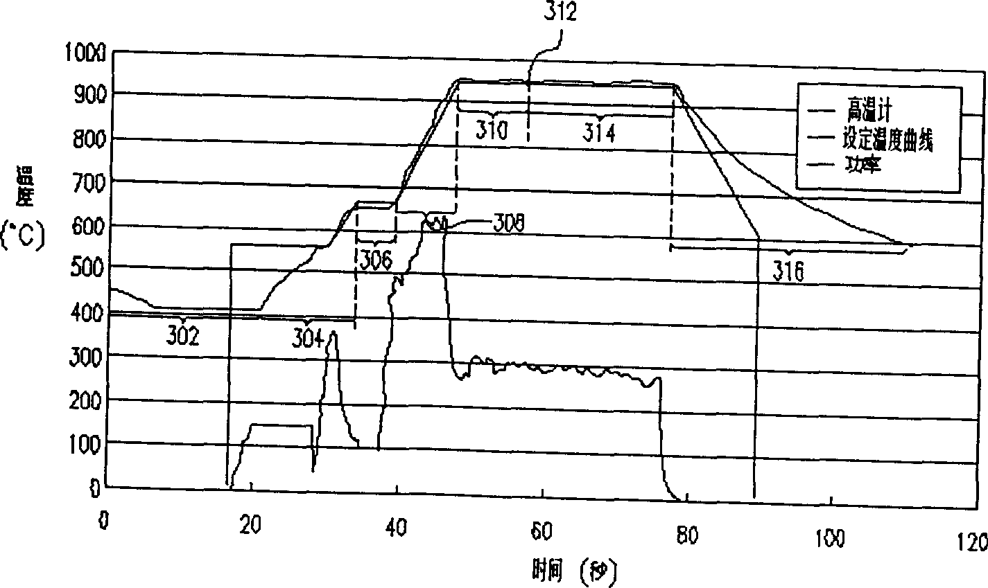
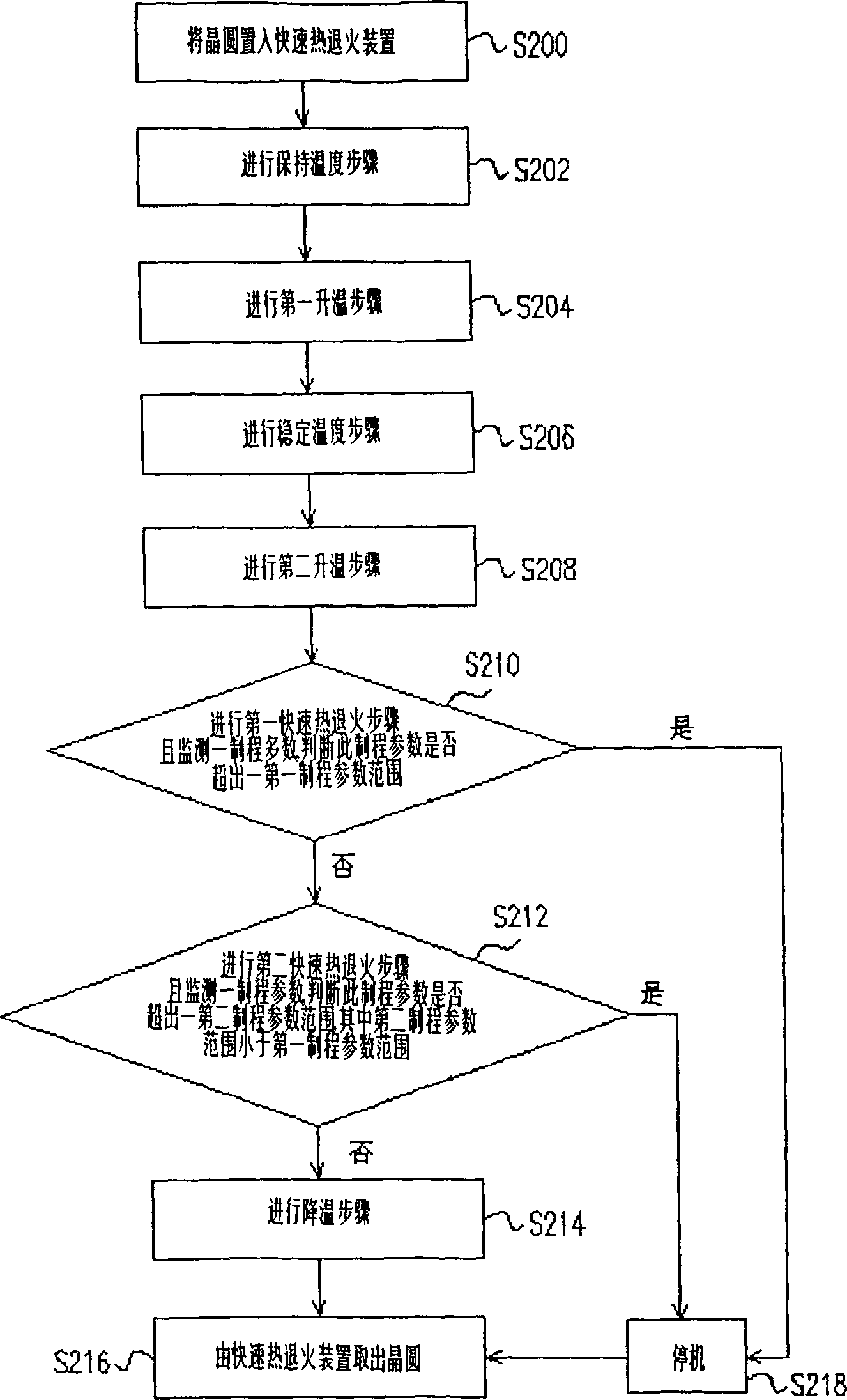
[0057] see figure 2 , image 3 as shown, figure 2 It is a schematic process flow diagram of a method for rapid thermal annealing of a semiconductor wafer according to a preferred embodiment of the present invention, image 3 It is a schematic diagram showing the temperature curve of a rapid thermal annealing process of a semiconductor wafer changing with the process time in a preferred embodiment of the present invention.
[0058] The method for rapid thermal annealing of the present invention comprises the following process steps:
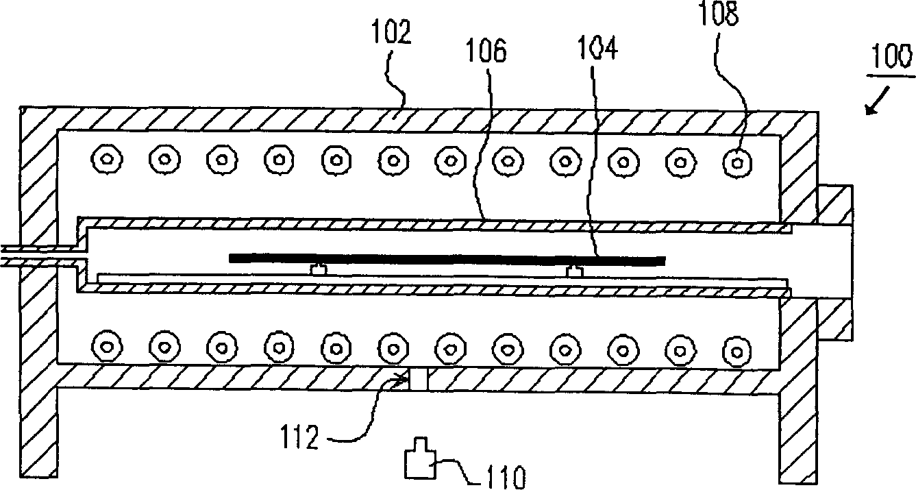
[0059] First, see figure 2 In step S200, the wafer (not shown) is loaded into the reaction chamber of the rapid thermal annealing device (device model: AST2800), wherein the rapid thermal anneal...
PUM
 Abstract
Description
Claims
Application Information
 - R&D Engineer
- R&D Manager
- IP Professional
- Industry Leading Data Capabilities
- Powerful AI technology
- Patent DNA Extraction
Browse by: Latest US Patents, China's latest patents, Technical Efficacy Thesaurus, Application Domain, Technology Topic, Popular Technical Reports.
© 2024 PatSnap. All rights reserved.Legal|Privacy policy|Modern Slavery Act Transparency Statement|Sitemap|About US| Contact US: help@patsnap.com