Stripping film
A film and copolymer technology, which is used in the field of peeling films, can solve the problems of high fluidity of thermoplastic resins and the inability of products to be extruded uniformly enough.
- Summary
- Abstract
- Description
- Claims
- Application Information
AI Technical Summary
Problems solved by technology
Method used
Image

Examples
Embodiment 1
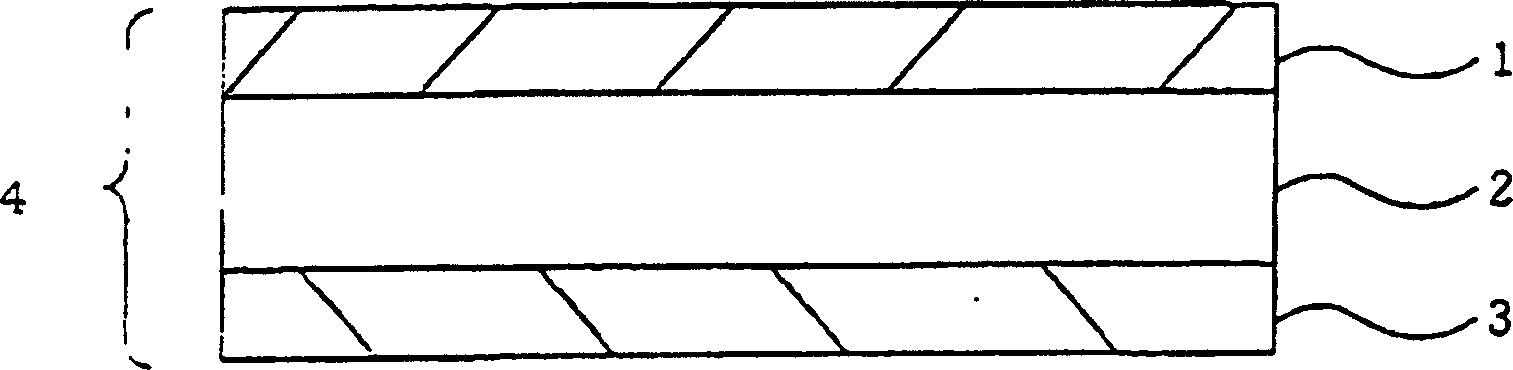
[0059] For the release film, an ETFE film (manufactured by Asahi Glass Company, Limited, AFLEX 12N, melting point: 265° C.) with a thickness of 12 μm was used as layer A, and a PET film (Toray Industries Inc., Lumilar X44, Melting point: 265° C.) as layer C. The layer B was prepared by extruding EVA (manufactured by Tosoh Corporation, Ultracene 541L, melting point: 95° C.). Then, layer A and layer C were bonded to both sides of layer B by extrusion lamination to prepare a release film having a thickness of 57 µm. Layer B has a thickness of 20 microns.
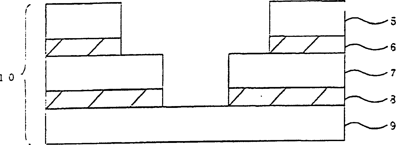
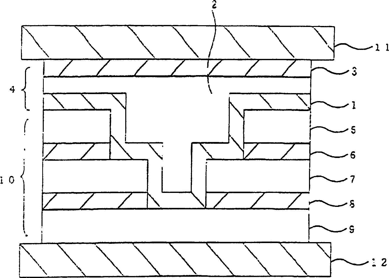
[0060] Using this release film, the layer A side of the release film is brought into contact with a multilayer printed circuit board, and the multilayer printed circuit board is subjected to compression molding. The obtained multilayer printed circuit board was excellent in surface smoothness at the concave-convex void portion, and substantially no leakage of the adhesive prepreg was observed.
Embodiment 2
[0062] A release film having a thickness of 57 µm was prepared in the same manner as in Example 1 except that EAA (manufactured by JPO Co., Ltd., ET184M, melting point: 86° C.) was used instead of EVA as Layer B. Layer B has a thickness of 20 microns. The multilayer printed circuit board was compression molded in the same manner as in Example 1. The obtained multilayer printed circuit board was excellent in surface smoothness at the concave-convex void portion, and substantially no leakage of the adhesive prepreg was observed.
Embodiment 3
[0064] A release film having a thickness of 57 µm was prepared in the same manner as in Example 1 except that EEA (manufactured by Mitsui-Dupont Polychemicals Co., Ltd., A701, melting point: 96° C.) was used instead of EVA as Layer B. Layer B has a thickness of 20 microns. The multilayer printed circuit board was compression molded in the same manner as in Example 1. The obtained multilayer printed circuit board was excellent in surface smoothness at the concave-convex void portion, and substantially no leakage of the adhesive prepreg was observed.
PUM
| Property | Measurement | Unit |
|---|---|---|
| melting point | aaaaa | aaaaa |
| thickness | aaaaa | aaaaa |
| thickness | aaaaa | aaaaa |
Abstract
Description
Claims
Application Information
 - R&D
- Intellectual Property
- Life Sciences
- Materials
- Tech Scout
- Unparalleled Data Quality
- Higher Quality Content
- 60% Fewer Hallucinations
Browse by: Latest US Patents, China's latest patents, Technical Efficacy Thesaurus, Application Domain, Technology Topic, Popular Technical Reports.
© 2025 PatSnap. All rights reserved.Legal|Privacy policy|Modern Slavery Act Transparency Statement|Sitemap|About US| Contact US: help@patsnap.com