Compound integrated circuit design verification method

A technology for integrated circuit and electronic design, applied in the field of design verification of composite integrated circuits, which can solve problems such as co-simulation and simulation that cannot run applications, long turnaround time, and difficulty in finding defects.

Inactive Publication Date: 2002-05-01
株式会社鼎新
View PDF3 Cites 5 Cited by
  • Summary
  • Abstract
  • Description
  • Claims
  • Application Information

AI Technical Summary

Problems solved by technology

Extended time co-simulation and simulation cannot run application
[0018] (2) It is difficult to find defects
[0019] (3) The cost of finding defects (manpower, time-market)
Today's design verification methods include different formats between the EDA environment and the tester environment, and therefore cannot complete design verification efficiently and accurately
Also, as mentioned above, today's design verification methodologies require in-system testing that involves hardware and software to run the design within the intended system, and requires significant feedback and interaction between the test environment and the design environment, resulting in longer turnaround times

Method used


Image

  • Compound integrated circuit design verification method
  • Compound integrated circuit design verification method
  • Compound integrated circuit design verification method

Examples


Embodiment Construction

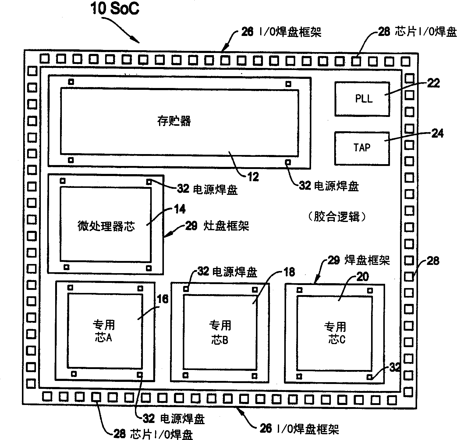
[0040] In prior patent applications owned by the same assignee of the present invention, event-based test systems are described in U.S. Patent Application Nos. 09 / 406,300 and 09 / 340,371 "Event based semiconductor testsystem," while Event-based design validation stations are described in / 428,746 "Method and apparatus for SoC design validation". Additionally, time scaling techniques are described in US Patent Application No. 09 / 286,226 "Scaling logic for Event Based Test System". All of these patent applications are hereby incorporated by reference herein.

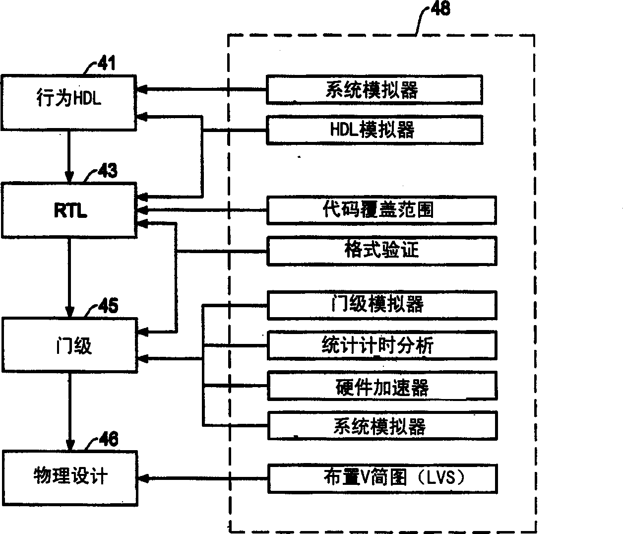
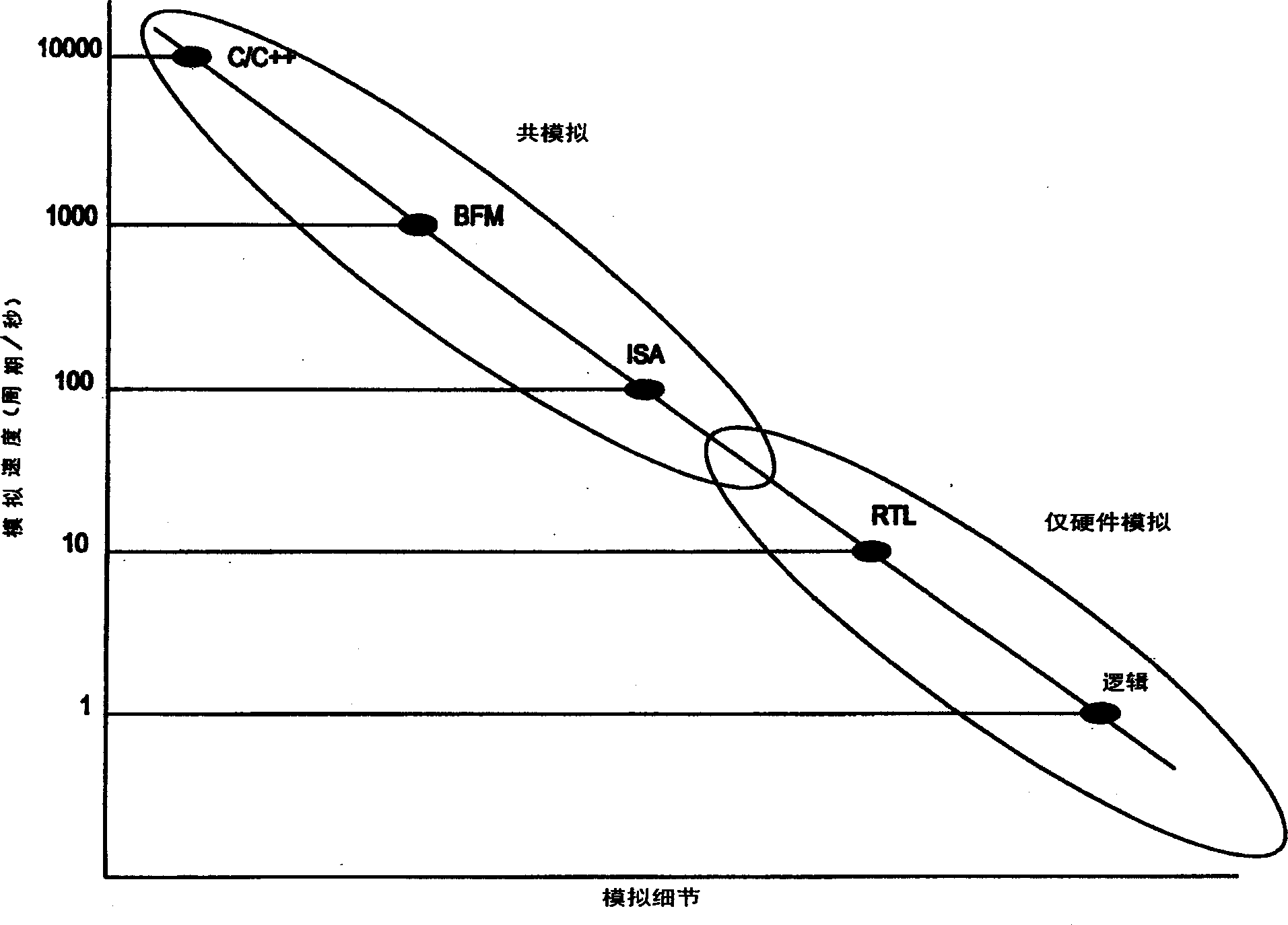
[0041] In the present invention, the inventors provide a concept of an integrated circuit design verification method using an event-based test system. More specifically, in the first embodiment, a design verification method using a silicon prototype is described, and in the second embodiment, a method without a silicon prototype is described. Both methods of the present invention are faster and less expensive than any cur...


PUM


Abstract

The method for design validation of complex IC with use of a combination of electronic design automation (EDA) tools and a design test station at high speed and low cost. The EDA tools and device simulator are linked to the event based test system to execute the original design simulation vectors and testbench and make modifications in the testbench and event based test vectors until satisfactory results are obtained. Because EDA tools are linked with the event based test system, these modifications are captured to generate a final testbench that provides satisfactory results.

Description

field of invention [0001] The present invention relates to a design verification method of a compound integrated circuit, more specifically, the present invention relates to a combination of an electronic design automation (EDA) tool and an event based test system (event based test system), high speed and low A method of cost-effectively evaluating and verifying the design of a complex integrated circuit, such as a system-on-chip. Background technique [0002] Currently, VLSI designs are described in blocks or sub-blocks using a high-level language such as Verilog or VHDL, and simulated using a behavioral gate-level Verilog / VHDL simulator. The purpose of this simulation is to check the functionality and characteristics of the design before it is fabricated into a silicon integrated circuit. [0003] Design verification is one of the most important and difficult tasks in compound integrated circuit design, because design errors cannot be found and eliminated without sufficie...

Claims


Application Information

Patent Timeline
Patent Type & Authority Applications(China)
IPC IPC(8): G01R31/28G01R31/3183G06F11/22G06F11/26G06F17/50
CPCG06F11/261G01R31/318314G06F17/5022G06F30/33
Inventor 矢元裕明罗基特·拉尤斯曼
Owner 株式会社鼎新
Why Eureka
Try Eureka