
Electronic parts

A technology of electronic components and internal components, applied in the direction of electrical components, electric solid devices, circuits, etc., can solve problems such as wiring disconnection, low productivity, and large processing technology

Inactive Publication Date: 2002-11-06
ORMON CORP
View PDF3 Cites 0 Cited by
  • Summary
  • Abstract
  • Description
  • Claims
  • Application Information

AI Technical Summary

Problems solved by technology

For this reason, a large number of machining processes are required, so the productivity is low
In addition, wiring may be disconnected due to vibration, etc., which causes a problem of low reliability

Method used


Image

  • Electronic parts
  • Electronic parts
  • Electronic parts

Examples


no. 1 example

[0180] On the upper surface of a sheet-like substrate with a thickness of 20 μm composed of a silicon wafer constituting the movable piece, an oxide film with a thickness of 1.4 μm, a bottom electrode with a thickness of 0.3 μm, a piezoelectric element with a thickness of 2 μm, and an upper electrode with a thickness of 0.3 μm are stacked sequentially. The electrode is a micro relay composed of a movable piece, the overall thickness is 24μm, the span is 4mm, and the width is 0.8mm, and the contact load and the deformation relative to the applied voltage are calculated. The calculation results are shown in Figs. 37A and 37B.

[0181] According to FIG. 37A and FIG. 37B, it can be seen that a specific contact pressure and displacement can be obtained only by controlling the voltage applied to the piezoelectric element.

no. 2 example

[0183] A heating layer with a depth of 3 μm is formed in the surface layer of a thin sheet-shaped substrate composed of a silicon wafer constituting a movable piece with a thickness of 20 μm, and an insulating oxide film with a thickness of 1.1 μm is formed on the upper surface of the heating layer. The micro relay composed of moving pieces has an overall thickness of 21.1μm, a span of 4mm, and a width of 0.8mm. Calculate the contact load and the deformation relative to the applied voltage. The calculation results are shown in Figs. 38A and 38B.

[0184] According to FIGS. 38A and 38B, it can be seen that only by controlling the applied voltage to adjust the heating value of the heating layer, a specific displacement and contact pressure can be obtained.

[0185] Matrix relays of fourteenth to seventeenth embodiments for achieving the second object will be described below with reference to FIGS. 39A to 45 .

[0186] As shown in FIGS. 39A and 41B , the fourteenth embodiment is...


PUM


Abstract

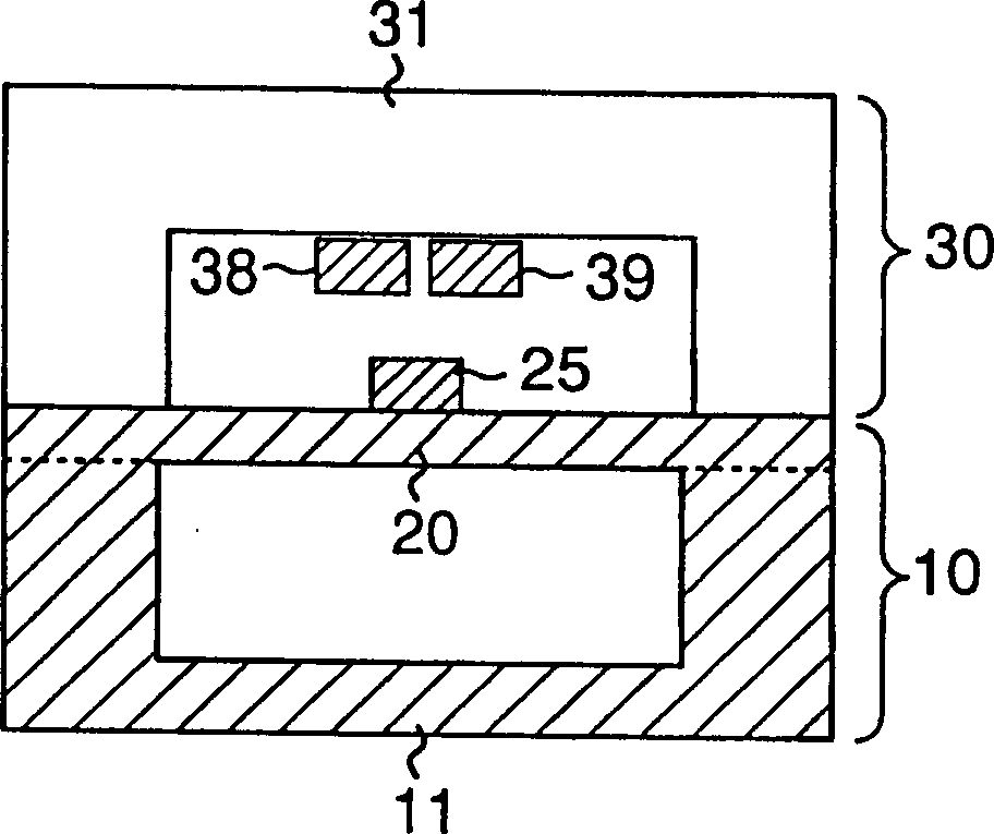
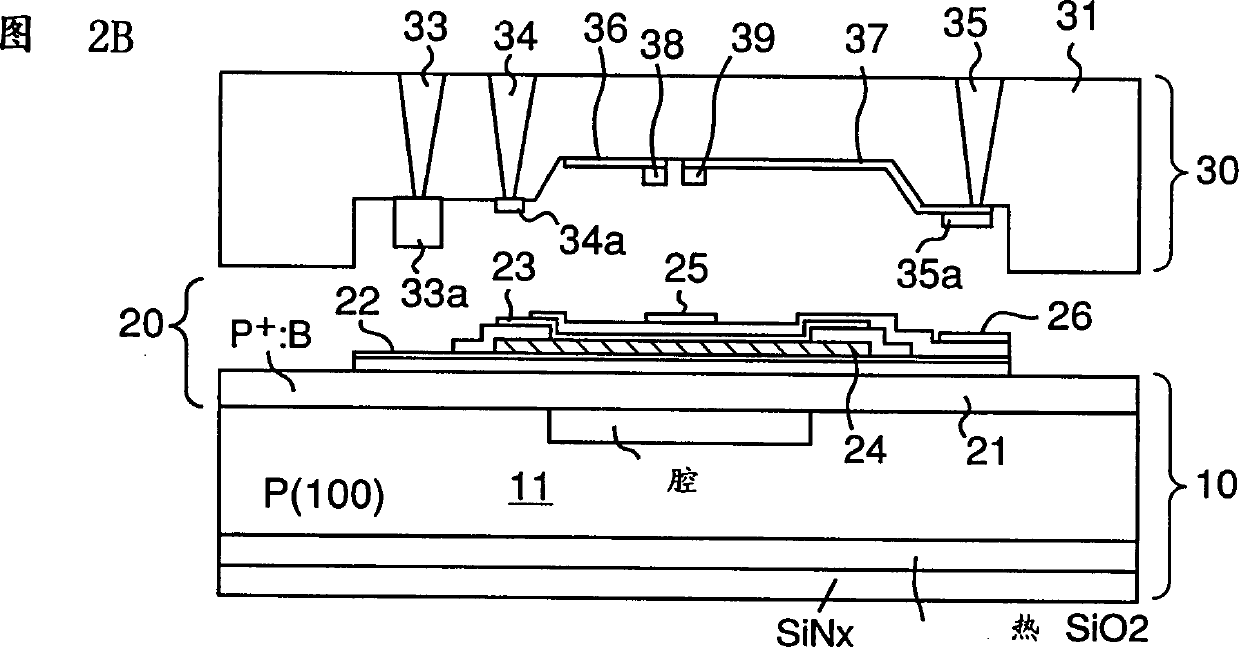
An electronic component that connects and integrates a cover made of glass material with a base made of silicon material, performs resin molding on an electronic device chip assembled with internal components on a substrate, thereby covering the cover with molding, exposing base bottom surface. By virtue of the through holes provided in the cover, the internal components are electrically connected with the external terminals of the substrate. A heat sink is provided on the bottom surface of the base exposed to the substrate. This makes it possible to obtain electronic parts that are prone to radiate heat, and can prevent malfunctions and changes in operating characteristics.

Description

[0001] The present invention is a divisional application of the invention patent application filed by Omron Corporation on August 27, 1997, entitled "Micro Relay and Its Manufacturing Method" and application number 97198654.1. technical field [0002] The present invention relates to electronic devices such as micro-relays, and more particularly to micro-relays, matrix relays and micro-relay chips having contacts that are opened and closed by bending a movable plate formed of a single-crystal lamellar substrate. Background technique [0003] Generally, as a relay, for example, there is an electromagnetic relay using an electromagnet. However, it is difficult to reduce the size of relays that must use mechanical parts. Also, the movable parts of the mechanical parts with a large inertial force suffer from unfavorable fatigue fractures and lack of durability. [0004] As a small-sized relay, there is also a semiconductor switching d...

Claims


Application Information

Patent Timeline
Patent Type & Authority Applications(China)
IPC IPC(8): B81B7/00H01H1/00H01H1/20H01H9/52H01H57/00H01H59/00H01H61/02H01H67/22H02N2/00
CPCB81B7/0077B81B2201/016B81B2207/095B81C2203/0118H01H1/0036H01H1/20H01H9/52H01H57/00H01H59/0009H01H61/02H01H67/22H01H2001/0042H01H2001/0084H01H2057/006H01H2061/006
Inventor 坂田稔中岛卓哉积知范藤原照彦竹内司
Owner ORMON CORP
Learn More