Dynamic matrix type display device having complementary capacitance on each pixel

A dynamic matrix and display device technology, applied in static indicators, nonlinear optics, instruments, etc., can solve the problem of lower aperture ratio and achieve the effect of preventing lamination and displacement

Inactive Publication Date: 2002-11-13
SANYO ELECTRIC CO LTD
View PDF0 Cites 17 Cited by
  • Summary
  • Abstract
  • Description
  • Claims
  • Application Information

AI Technical Summary

Problems solved by technology

Therefore, the problem of lower aperture ratio will become larger

Method used


Image

  • Dynamic matrix type display device having complementary capacitance on each pixel
  • Dynamic matrix type display device having complementary capacitance on each pixel
  • Dynamic matrix type display device having complementary capacitance on each pixel

Examples


no. 1 Embodiment

[0063] In the dynamic matrix LCD related to the first embodiment, there is a pixel portion in which each TFT is provided on a first substrate, and even a driving portion for driving the pixel portion is formed around the pixel portion on the same substrate .

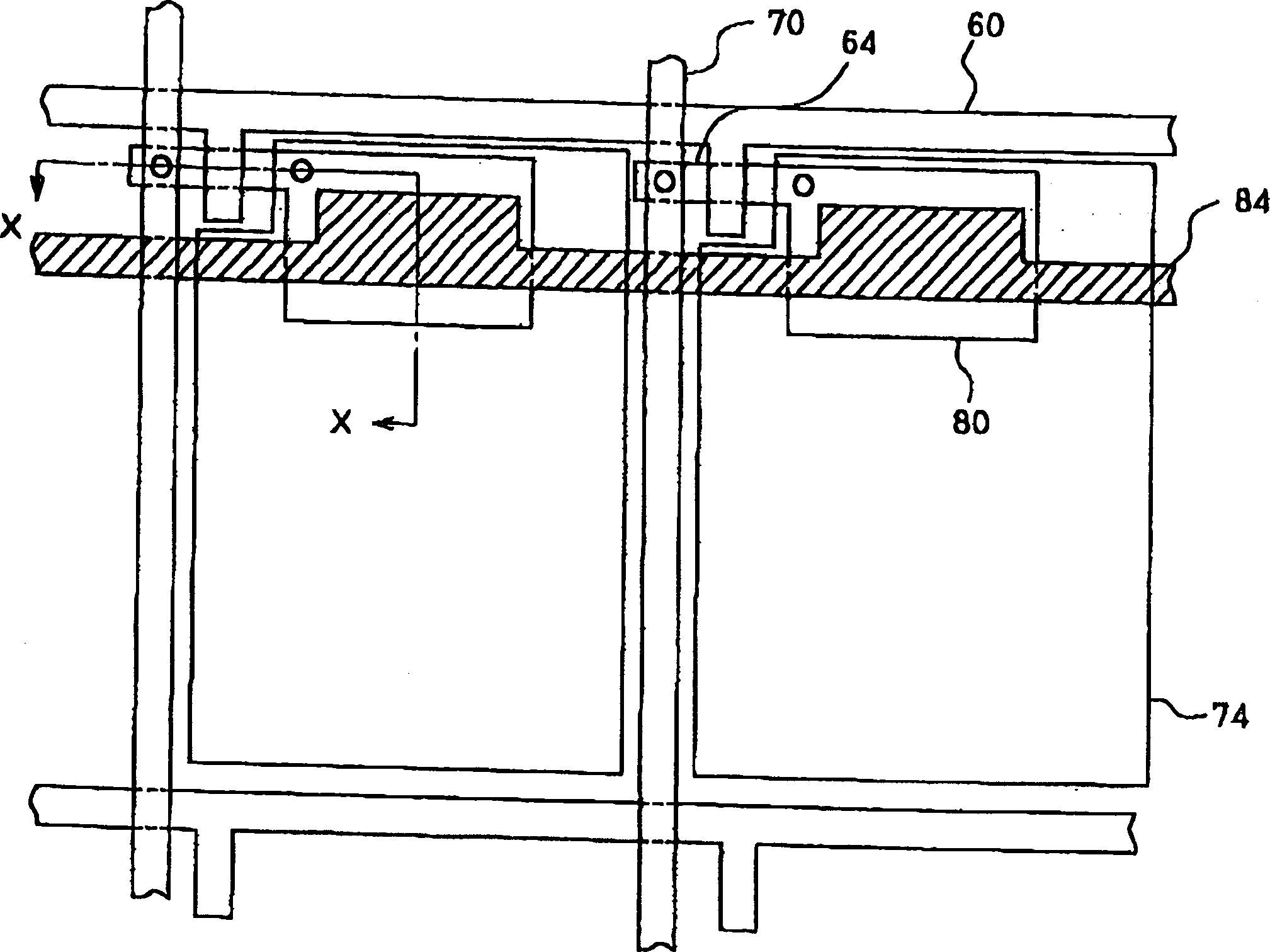
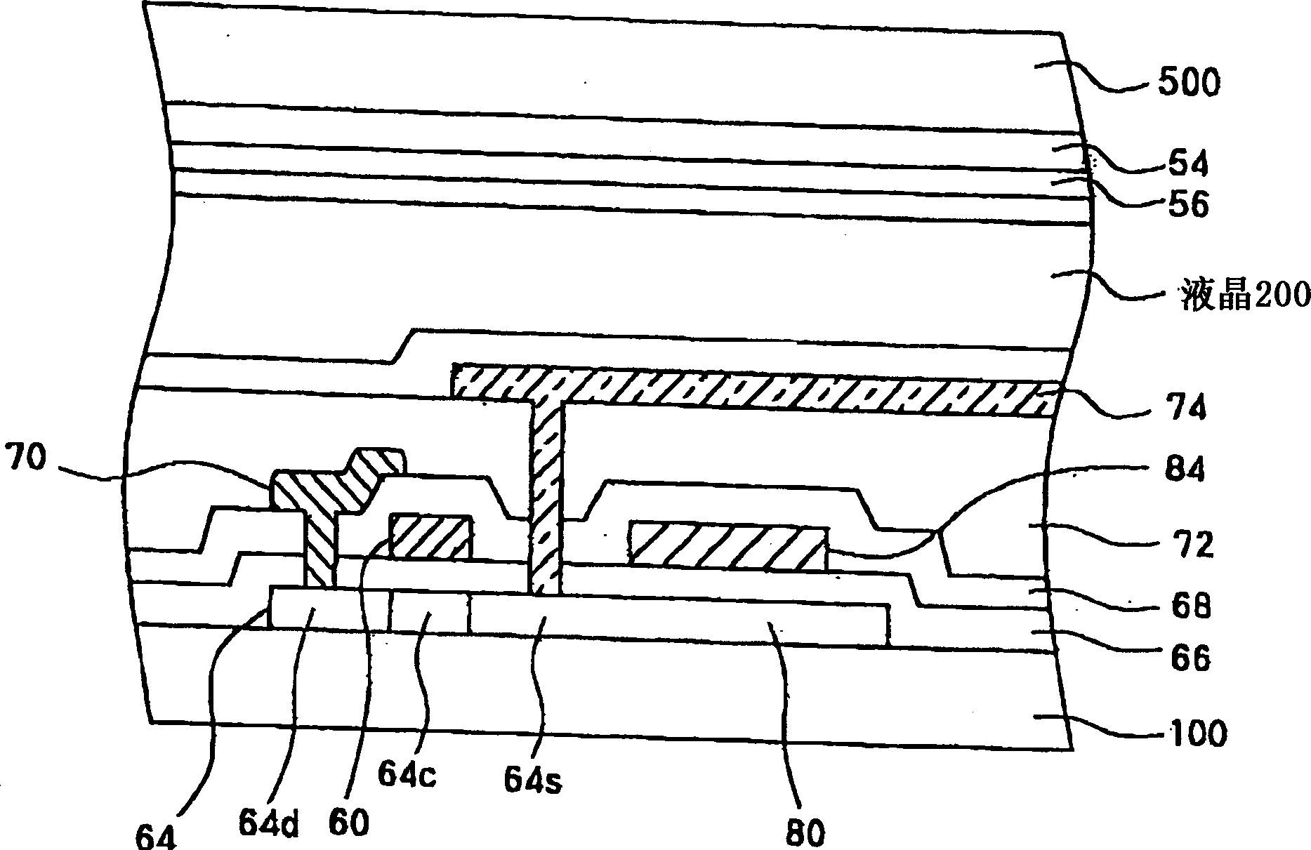
[0064] First, the pixel portion will be described. Figure 4 , Shows the planar structure of the pixel portion of the LCD related to the first embodiment, Figure 5 , Is the display edge Figure 4 The schematic cross-sectional structure of the LCD at the A-A line position, Figure 6 , Is the display edge Figure 4 The cross-sectional structure on the first substrate at the position of the B-B line.

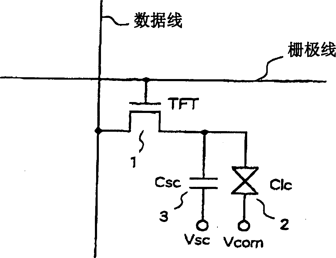
[0065] The equivalent circuit of each pixel is the same as that of FIG. 1, on the first substrate 100, such as Figure 4 As shown, the pixel electrodes 24 are arranged in a matrix, corresponding to each pixel electrode 24, and are provided with a top gate type TFT1 and an auxiliary capacitor 3 (Csc). In each pixel, the active la...

no. 2 Embodiment

[0100] Picture 12 , Is a plane structure for displaying display pixels of the dynamic matrix LCD related to the second embodiment. And along this Picture 12 The schematic cross-sectional structure of the LCD at the position of the A-A line is the same as the above Figure 5 the same. Figure 13 , Is the display edge Picture 12 The cross-sectional structure on the first substrate at the B-B line position. In addition, the same symbols are attached to the structures corresponding to the drawings described below, and the description is omitted.

[0101] The auxiliary capacitor Csc is the first electrode 30 and the second electrode 32, sandwiching the insulating layer 12 to form an overlapping area. Although this point is the same as the above embodiment, in the second embodiment, the first electrode 30 and the TFT The active layer 14 is integrally formed, and in order to make the first electrode 30, the active layer 14 can be formed along the data line 22 passing through the edge...

no. 3 Embodiment

[0112] Figure 14 , A schematic planar structure in each display pixel of the dynamic matrix liquid crystal display device related to the third embodiment. However, for the pixel electrode 24, the description is omitted for easy viewing of the drawing. In addition, Figure 15 , Is the display edge Figure 14 The cross-sectional structure on the first substrate at the position of the C-C line. Common symbols are attached to the parts that are common to the above-mentioned first and second embodiments.

[0113] In the second embodiment described above, in order to prevent coupling, the layout is performed so that the first electrode of the auxiliary capacitor integrated with the TFT active layer does not overlap the data line 22. In contrast, in the third embodiment, the first electrode 30 of the auxiliary capacitor overlaps the data line formation area, and in order to prevent coupling, in the overlap area with the first electrode 30 and the data line, A conductive sealing layer i...


PUM


Abstract

A dynamic matrix display device in which each pixel has a top gate type TFT, an auxiliary capacitor Csc, and a liquid crystal capacitor C1c in a pixel portion, the first electrode (30) of the auxiliary capacitor Csc is also used by the TFTp-Si active layer (14), and the second 2. The electrode (32) is formed on the lower layer of the active layer (14) and holds the insulating layer (12) therebetween so as to overlap at least a part of the active layer (14). In the case of a built-in driving part, the driving part TFT and the pixel part TFT are both of the top gate type, and the active layer (140) and the active layer (14) are made of the same material, and an insulating layer is provided under the active layer (140). (12) and a conductive layer (32D) made of the same material as the second electrode (32). In the pixel part, the reduction of the aperture ratio will be prevented and the auxiliary capacitance will be formed at the same time, and the polycrystallization annealing conditions of the active layer can be the same through the TFT in the pixel part and the TFT in the driving part, and TFTs with consistent characteristics can be obtained.

Description

Technical field [0001] The present invention relates to a dynamic matrix display device including thin film transistors in each pixel. Background technique [0002] Flat-panel displays such as liquid crystal display devices (hereinafter referred to as LCD) have low power consumption because they can be thinned, miniaturized, and lightweight. LCDs, such as mobile information devices, have been used in most devices as various The display part of the machine. In LCDs, etc., thin film transistors are provided in each pixel as a switching element, which is called a dynamic matrix type. Since this panel can reliably maintain the display content of each pixel, it can be used to achieve high-precision display and high-quality display. On the display device. Figure 1 shows the equivalent circuit for dynamic matrix LCD pixels. Each pixel is equipped with a thin film transistor 1 (TFT) connected to the gate line and the data line, and when the TFT is turned on by the selection signal output...

Claims


Application Information

Patent Timeline
Patent Type & Authority Applications(China)
IPC IPC(8): G02F1/136G02F1/1362
CPCG02F1/136213G02F1/136
Inventor 米田清宫岛康志横山良一山田努
Owner SANYO ELECTRIC CO LTD
Why Eureka
Try Eureka