Scanning structure in display, method for driving display and its producing method

A technology for scanning drivers and displays, used in semiconductor/solid-state device manufacturing, static indicators, instruments, etc., can solve problems such as image uniformity deterioration, current difference, etc.

Inactive Publication Date: 2003-01-01
LG DISPLAY CO LTD
View PDF0 Cites 5 Cited by
  • Summary
  • Abstract
  • Description
  • Claims
  • Application Information

AI Technical Summary

Problems solved by technology

As a result, a current difference is generated between the two parts, whereby the uniformity of the image deteriorates

Method used


Image

  • Scanning structure in display, method for driving display and its producing method
  • Scanning structure in display, method for driving display and its producing method
  • Scanning structure in display, method for driving display and its producing method

Examples


Embodiment Construction

[0048] Reference will now be made in detail to the preferred embodiments of the invention, examples of which are illustrated in the accompanying drawings. Where possible the same reference numbers refer to the same or like parts throughout the drawings.

[0049] A scanning structure and a manufacturing method thereof according to the present invention will be explained with reference to the accompanying drawings.

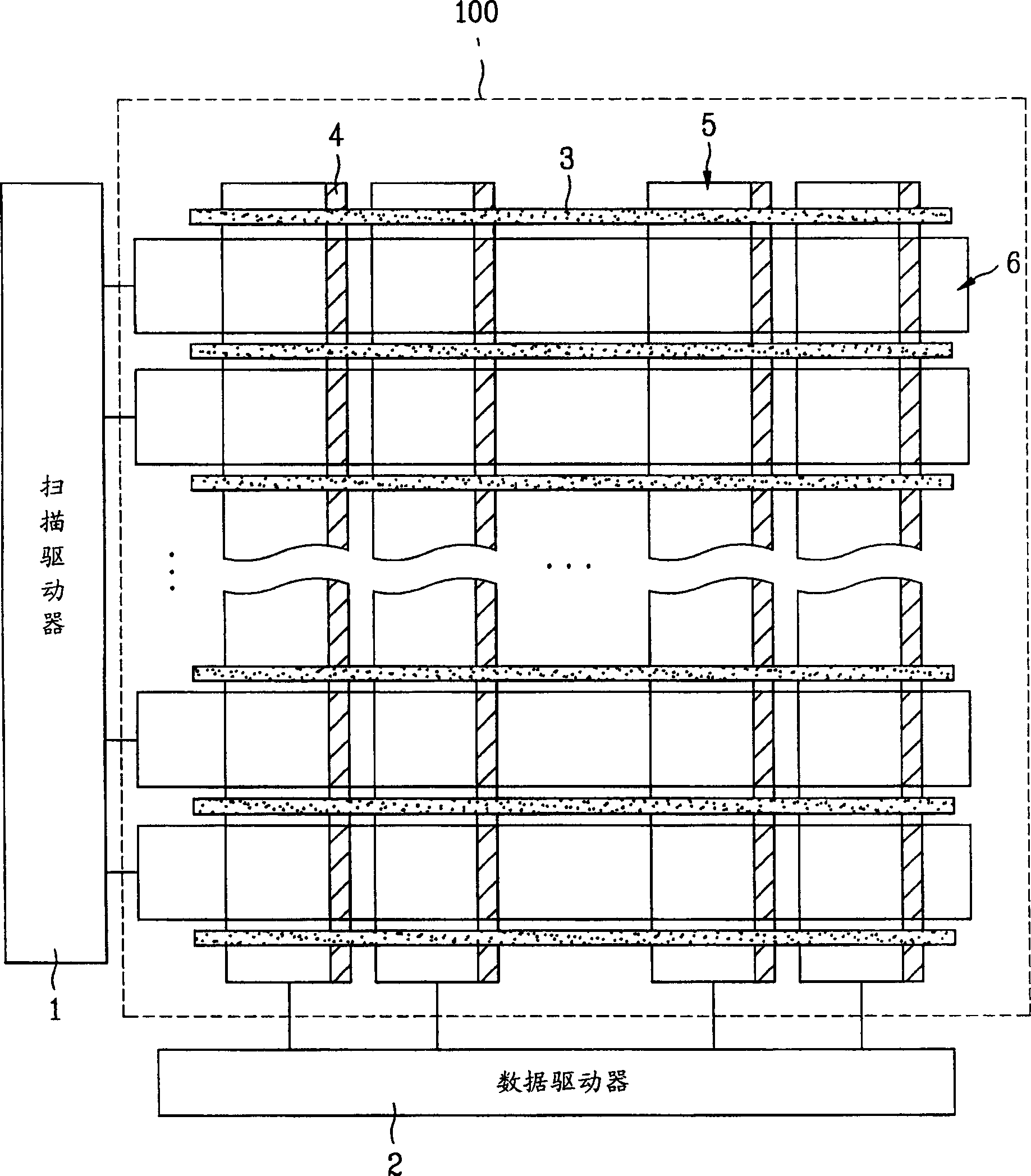
[0050] image 3 is a diagram showing the scanning structure of the display according to the first embodiment of the present invention.

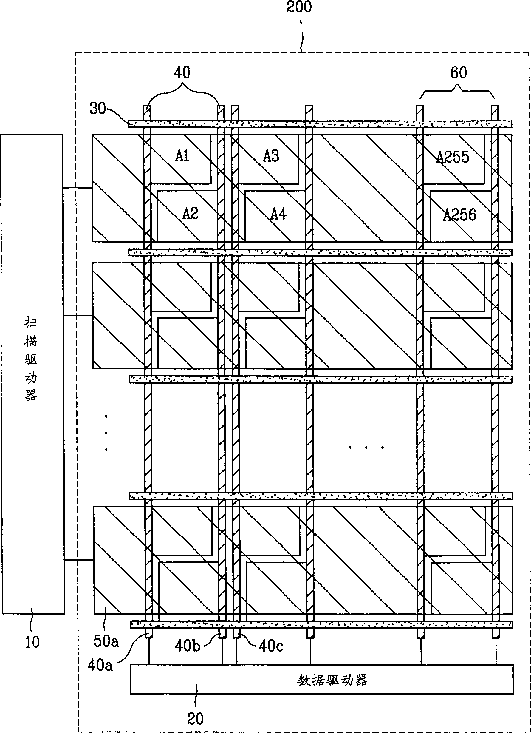
[0051] Such as image 3 As shown, the display according to the present invention includes an organic EL panel 200 , a data driver 20 and a scan driver 10 .

[0052] At this time, a plurality of data lines 60 and scan lines 50 a form a matrix on the organic EL panel 200 . That is, the plurality of data lines 60 cross the plurality of scanning lines 50a, thereby forming a plurality of pixels (units for emitting light) of the organi...


PUM


Abstract

A scan structure of a display device, a method for driving the display device, and a method for manufacturing the same is disclosed, which is for physically decreasing a duty in half, maintaining uniform picture quality. In the display device having a plurality of data lines formed in one direction, a plurality of scan lines formed in perpendicular to the plurality of data lines, a plurality of pixels are formed, which are connected to the plurality of data lines in each scan line, so that the total scan time is increased in proportion to the number of the pixels in each scan line.

Description

technical field [0001] The present invention relates to displays, and more particularly to scanning structures in displays for reducing the power of passive panels, and to methods of driving displays, and methods of manufacturing displays. Background technique [0002] Recently, flat panel displays have been rapidly developed. In particular, flat panel displays such as liquid crystal displays (LCDs) have replaced cathode ray tubes (CRTs). Also, flat panel displays such as plasma display panels (PDPs), vacuum fluorescent displays (VFDs), field emission displays (FEDs), light emitting diodes (LEDs), and electroluminescence (ELs) are being actively researched. [0003] The flat display can be used in various fields, among which the flat display has excellent visual experience, high resolution and simplified processing steps. [0004] With the trend of large-size and high-resolution flat-panel displays, larger currents are used in driving circuits to d...

Claims


Application Information

Patent Timeline
Patent Type & Authority Applications(China)
IPC IPC(8): G02F1/133G09F9/30G09G3/20G09G3/30G09G3/32H01L27/32H01L51/50H05B33/10H05B33/26
CPCH01L27/3288G09G2300/0439G09G2310/0205G09G3/3216H10K59/179G09G3/20
Inventor 金学洙
Owner LG DISPLAY CO LTD
Why Eureka
Try Eureka