Contact structure having contact block

A technology of contact structure and contactor, which is applied in the direction of contact parts, connections, fixed connections, etc., and can solve problems such as contact pressure, contact resistance and bandwidth influence

Inactive Publication Date: 2003-02-19
株式会社鼎新 +1
View PDF0 Cites 25 Cited by
  • Summary
  • Abstract
  • Description
  • Claims
  • Application Information

AI Technical Summary

Problems solved by technology

Therefore, during the temperature change, the contact position will also change, which will adversely affect the contact pressure, contact resistance and bandwidth

Method used


Image

  • Contact structure having contact block
  • Contact structure having contact block
  • Contact structure having contact block

Examples


Embodiment Construction

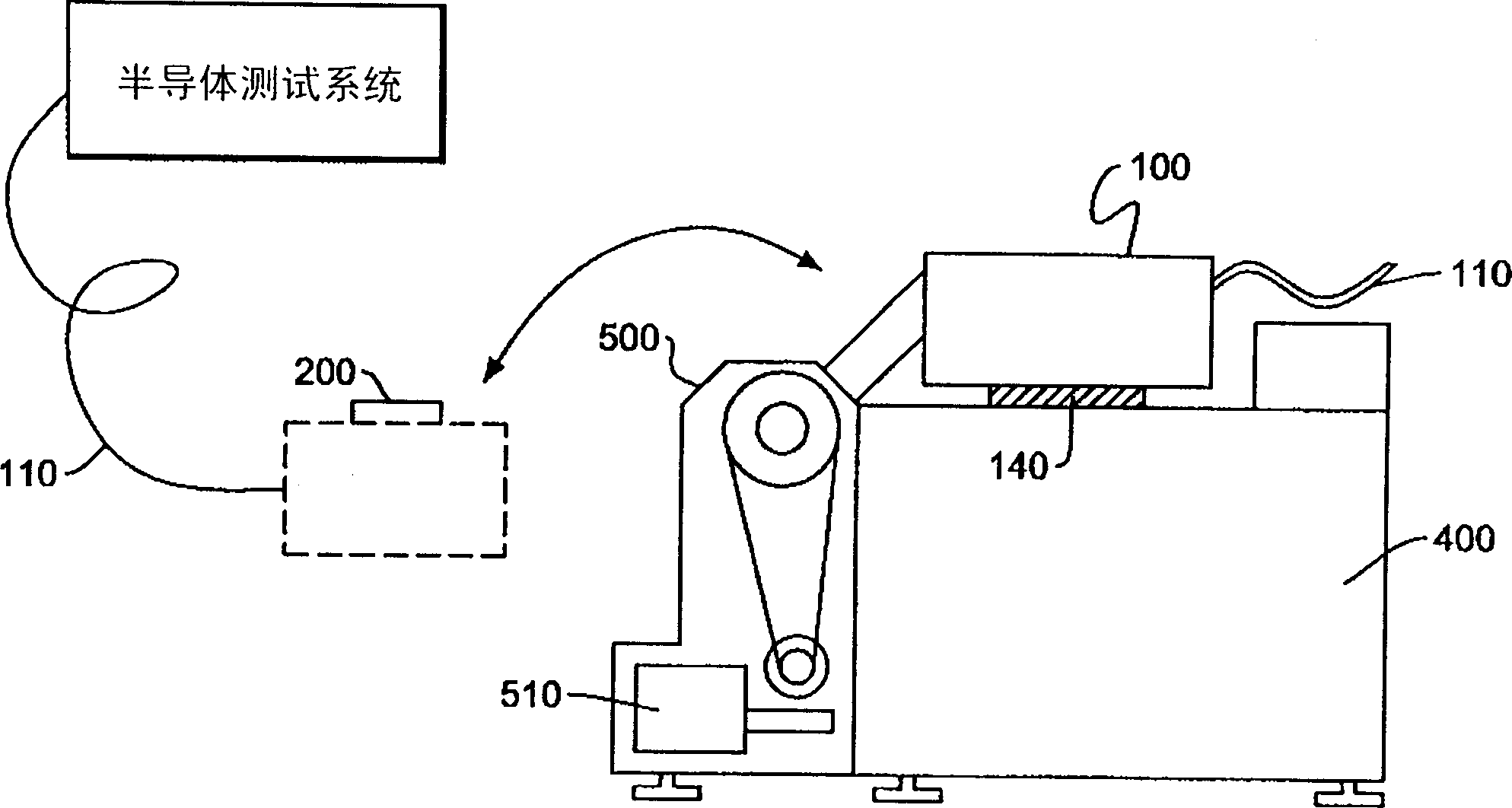
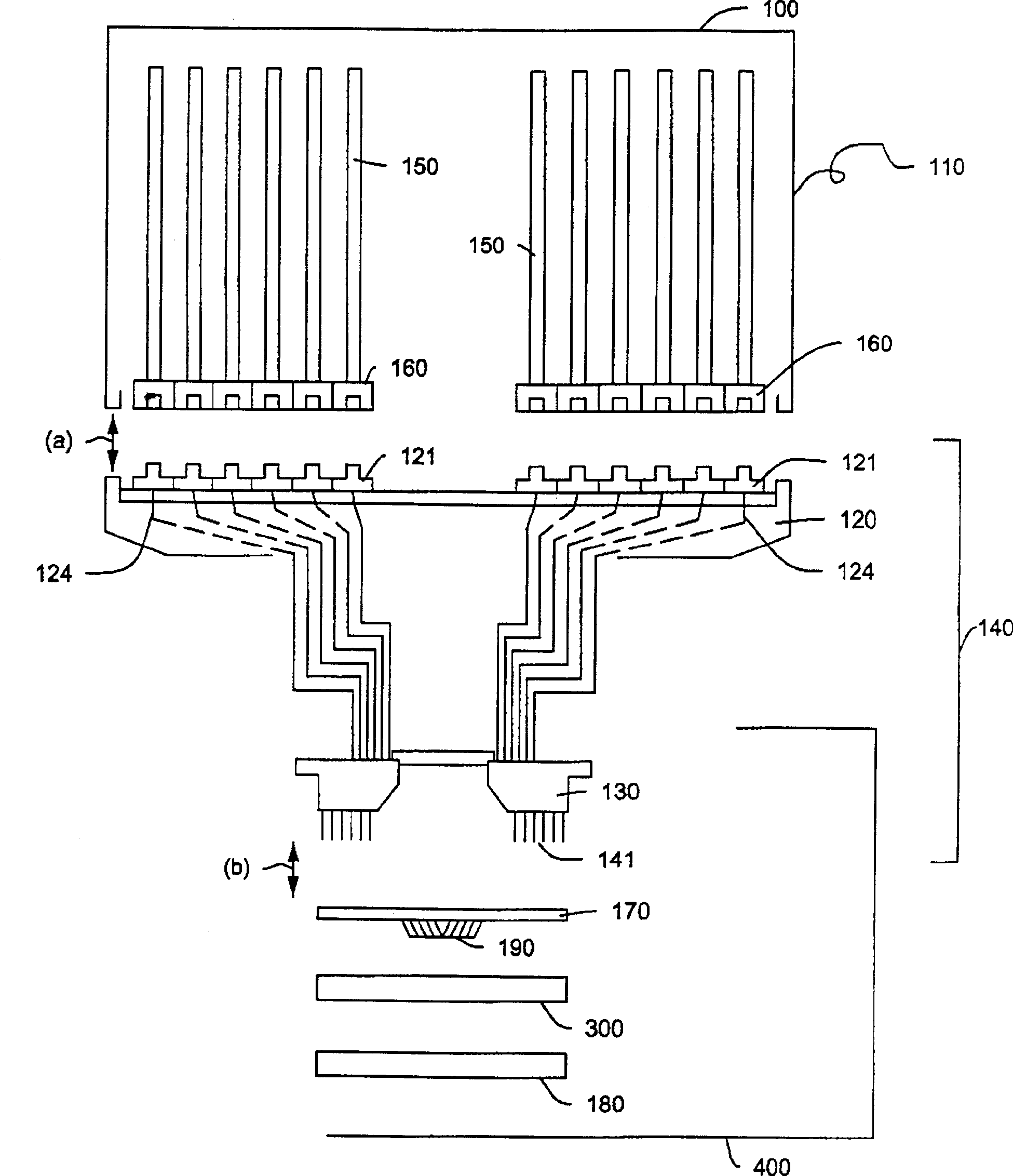
[0038] A first embodiment of the contact structure of the present invention is shown in Fig. 5 and Figure 6 Among them, it includes a plurality of plate-shaped contacts 30 as a whole, and the contactor is composed of a plurality of wires 35 , a dielectric layer 36 , a ground layer 37 and a plurality of contact bumps 31 fixed on the wires 35 . exist Figure 6 , the contactor 30 is fixed on the contact substrate 20 . The plate contact 30 is preferably formed by a tape automated bonding (TAB) technique used in the electronics industry. Tape Automated Attachment Process (TAB) is usually used to roll up semiconductor wafers when thinner housings are required. In the present invention, this TAB technique is used to create an impedance-matched contact structure to achieve higher frequency bandwidth.

[0039] When this TAB technique is used in the present invention, a set of contacts having a plurality of contacts mounted on a dielectric substrate further mounted on a ground plane...


PUM


Abstract

A contact structure for creating the electric connection with the object on the substrate to be tested has the TAB form using spherical contactor as contact point. It has more contactors formed by the conductive line on the grounding layer and passing through the dielectric layer, and a substrate for fixing said contactors on it and electrically connecting them to external part. The said conductive line is a microstrip line with a hard boss at its end. When the contact structure is pressed on the substrate to be tested, it is curved to contact with the said boss with a friction effect.

Description

(1) Technical field [0001] The present invention relates to contact structures for establishing electrical connections with contact objects such as contact pads or leads of electronic circuits or devices, and more particularly, the present invention relates to contact structures for use in a probe card that probes Pin boards are used to test semiconductor wafers, semiconductor chips, packaged semiconductor devices, component sockets, and printed circuit boards with improved bandwidth, lead spacing, and contact performance and reliability. (2) Background technology [0002] When testing high-density and high-speed electrical devices, such as LSI and VLSI circuits, high-performance contact structures such as probe contactors or test contactors must be used. The contact structure of the present invention is not only applied to the testing and burning of semiconductor wafers and chips, but also includes the testing and burning of packaged semiconductor devices, printed circuit b...

Claims


Application Information

Patent Timeline
Patent Type & Authority Applications(China)
IPC IPC(8): G01R1/073G01R31/26H01R12/30H01R12/50H01R13/03
Inventor 西奥多·A·库利蒂姆·弗雷什
Owner 株式会社鼎新
Why Eureka
Try Eureka