
Display board and liquid crystal display with the same

A technology of liquid crystal display and display substrate, which is applied to LCD. field, can solve the problem that the organic insulating layer cannot be removed

Inactive Publication Date: 2003-04-23
SAMSUNG DISPLAY CO LTD
View PDF0 Cites 14 Cited by
  • Summary
  • Abstract
  • Description
  • Claims
  • Application Information

AI Technical Summary

Problems solved by technology

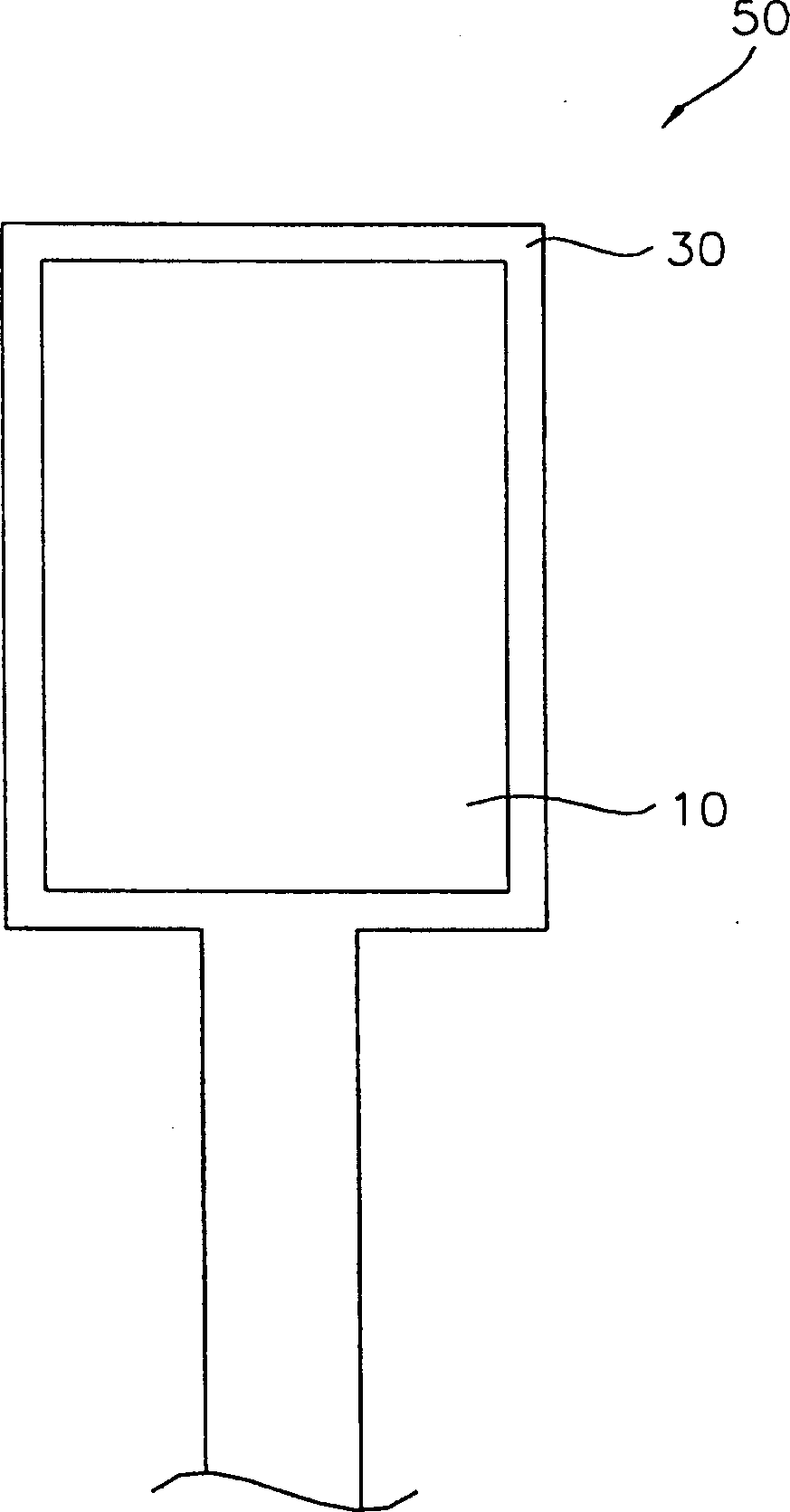
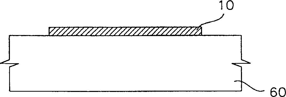
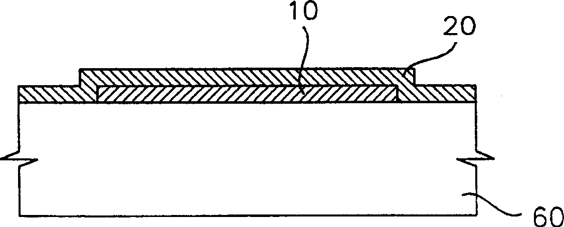
Therefore, the organic insulating layer 30 cannot be completely removed from the portion where the gate pad 10 is formed.

Method used


Image

  • Display board and liquid crystal display with the same
  • Display board and liquid crystal display with the same
  • Display board and liquid crystal display with the same

Examples


Embodiment Construction

[0043] Hereinafter, the present invention will be described in detail with reference to the accompanying drawings. Figure 4 is a perspective view showing an LCD according to a preferred embodiment of the present invention.

[0044] see Figure 4 , the LCD 600 includes a liquid crystal display panel 300 and a gate PCB 400 and a data PCB 500 for applying driving signals to the liquid crystal display panel 300 .

[0045] The liquid crystal display panel 300 includes a TFT substrate 200 , a color filter plate 100 and a liquid crystal (not shown) injected between the two substrates 200 and 100 .

[0046] The TFT substrate 200 is a transparent glass plate on which matrix type TFTs (not shown) are formed. The source electrode ( 214 in FIG. 8E ) of the TFT is connected to the data line 220 , and the gate electrode ( 211 in FIG. 8E ) is connected to the gate line 230 . In addition, a pixel electrode (not shown) composed of a transparent conductive substrate ITO is formed as a drain...


PUM


Abstract

A displaying substrate and a liquid crystal display device having the same are disclosed. A pad portion formed on the displaying substrate has a plurality of via holes for exposing a pad metal layer. A width of the via hole is smaller than a diameter of a conductive particle. Where the width of the via hole is larger than the diameter of the conductive particle, a depth of the via hole is smaller than the diameter of the conductive particle. Thus, a driving failure which may occur in the pad portion is prevented while maintaining a deformation ratio of the conductive particle at about 20~60%, thereby enhancing a connecting force between the pad portion and a circuit substrate.

Description

technical field [0001] The present invention relates to a display substrate and a liquid crystal display (hereinafter referred to as "LCD") having the substrate, in particular to a display substrate formed with a solder joint portion capable of enhancing contact characteristics with a circuit board for applying electrical signals to the display substrate And an LCD including the display substrate. Background technique [0002] In recent years, information processing applications have rapidly evolved to have various forms and functions, and faster information processing speeds. The information in the form of electrical signals processed in such information processing applications requires a display that acts as an interface. [0003] There has been developed a flat panel type display which is lighter in weight and smaller in size than the CRT type display and has advantages of realizing full color and high resolution. LCD is currently the most popular ...

Claims


Application Information

Patent Timeline
Patent Type & Authority Applications(China)
IPC IPC(8): G02F1/1345G02F1/13G02F1/133G02F1/1362G09F9/00G09F9/30G09F9/35H05K1/11H05K3/32H05K3/36
CPCG02F1/13452H05K1/113H05K3/361H05K1/115H05K2201/0979G02F1/13458H05K2201/09509H05K3/323H05K2201/10136G02F1/133
Inventor 吴元植俞炯硕尹胄永赵源九
Owner SAMSUNG DISPLAY CO LTD
Learn More