

Three-D integrated memory
A three-dimensional integration and three-dimensional storage technology, applied in the fields of electric solid-state devices, semiconductor devices, semiconductor/solid-state device components, etc., can solve the problems of 3D-M read and write speed, yield programmability, etc.
- Summary
- Abstract
- Description
- Claims
- Application Information
AI Technical Summary
Problems solved by technology
Method used
Image

Examples
specific Embodiment approach 1 3
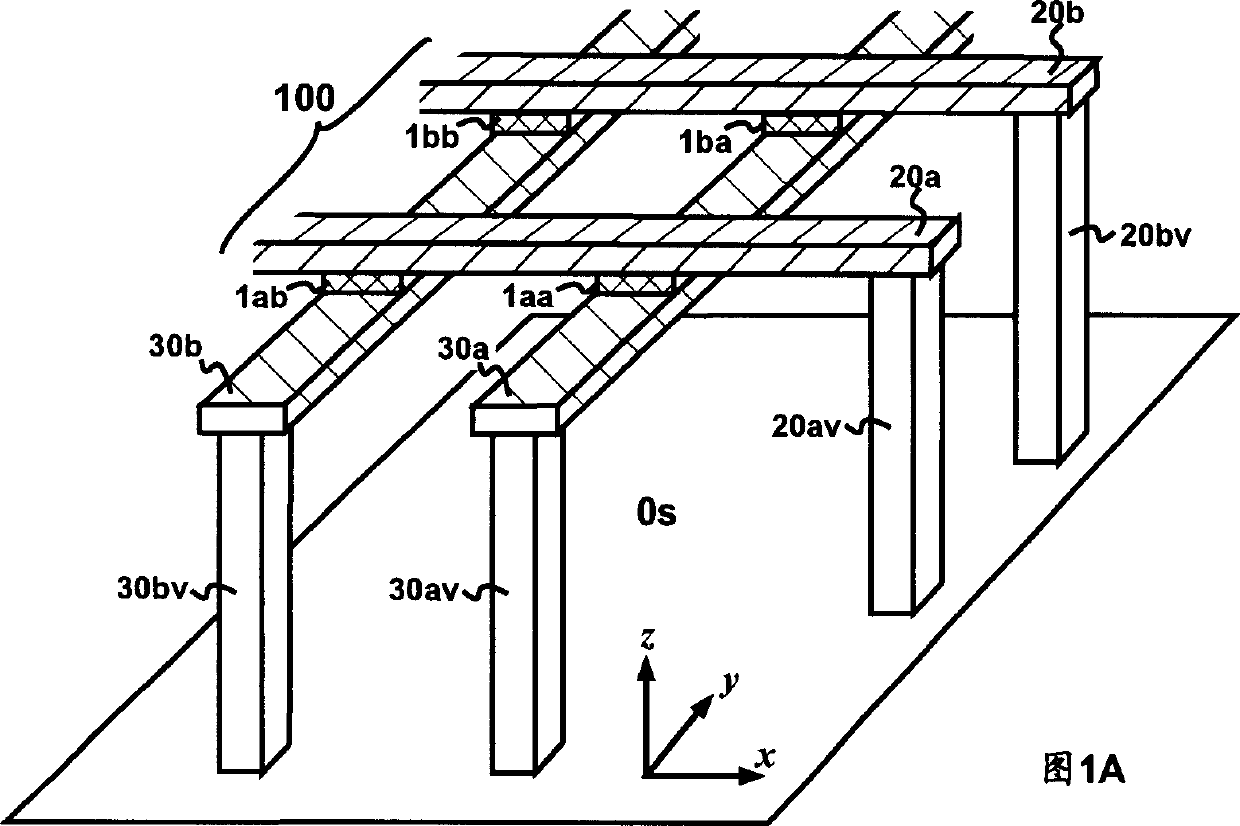
[0041] DETAILED DESCRIPTION 1. Three-dimensional integrated memory (3DiM)
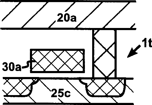
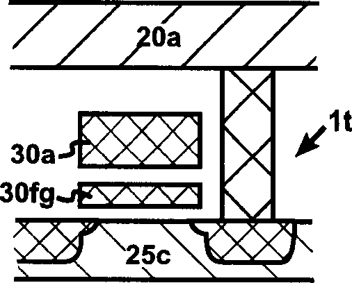
[0042] FIG. 2A is a cross-sectional view of a three-dimensional integrated memory (3DiM). 3DiM integrates the 3D-M array 0A and the substrate circuit 0s. The 3D-M array OA includes one or more three-dimensional storage layers 100 . Each three-dimensional storage layer 100 contains multiple address selection lines (20a, 30i...) and multiple 3D-M elements (1ai...). These address select lines contain metallic material and / or doped semiconductor material. The transistor 0T on the substrate and its interconnection 0I (0Ia, 0Ib...) constitute the substrate circuit 0s. From a circuit point of view, the substrate circuit OS includes a substrate integrated circuit OSC and address decoders 12, 18 / 70 (FIG. 2B). These address decoders 12, 18 / 70 provide address decoding for the 3D-M array OA. Contact vias (20av...) provide electrical connections for address select lines (20a...) and sub...
PUM
 Abstract
Description
Claims
Application Information