Double-fluid jet nozzle for cleaning, cleaner and method for making semiconductor using same

A dual-fluid nozzle and cleaning device technology, which can be used in liquid ejection devices, semiconductor/solid-state device manufacturing, and ejection devices, etc., can solve problems such as re-attachment, easy-to-adhesion particles, and fine pattern damage.

Inactive Publication Date: 2003-05-21
MITSUBISHI ELECTRIC CORP
View PDF1 Cites 7 Cited by
  • Summary
  • Abstract
  • Description
  • Claims
  • Application Information

AI Technical Summary

Problems solved by technology

[0005] Even if most of the pollutants and liquid and gas are discharged from the exhaust port 53, a part of the liquid is atomized, and the pollutants originally attached to the surface of the semiconductor wafer 10 together with the particles originally contained in the gas are The upper part of the cleaning chamber 52 is dispersed, and there is a problem of reattaching to the surface of the semiconductor wafer with a certain probability
[0006] Furthermore, in prior art cleaning with two-fluid nozzles and even equipped with the cleaning device of the nozzle, since most of the injected gas is directly blown to the surface to be cleaned (hereinafter referred to as "cleaned surface") Therefore, the surface to be cleaned is in a dry state, and particles are easy to adhere to
And, as mentioned above, when the pollutants to be removed were diffused in the cleaning chamber 52, the chances of the particles originally contained in the gas to impact the surface to be cleaned increased, and there was also the problem that the particles were attached to the surface to be cleaned.
In particular, when fine patterns are formed on the surface of a semiconductor substrate, etc., the fine patterns may be damaged due to the impact of particles in the gas.
[0007] In addition, since the exhaust port 53 is connected to the bottom of the object to be cleaned, it is difficult for liquid and gas to be discharged quickly.

Method used


Image

  • Double-fluid jet nozzle for cleaning, cleaner and method for making semiconductor using same
  • Double-fluid jet nozzle for cleaning, cleaner and method for making semiconductor using same
  • Double-fluid jet nozzle for cleaning, cleaner and method for making semiconductor using same

Examples


Embodiment 3

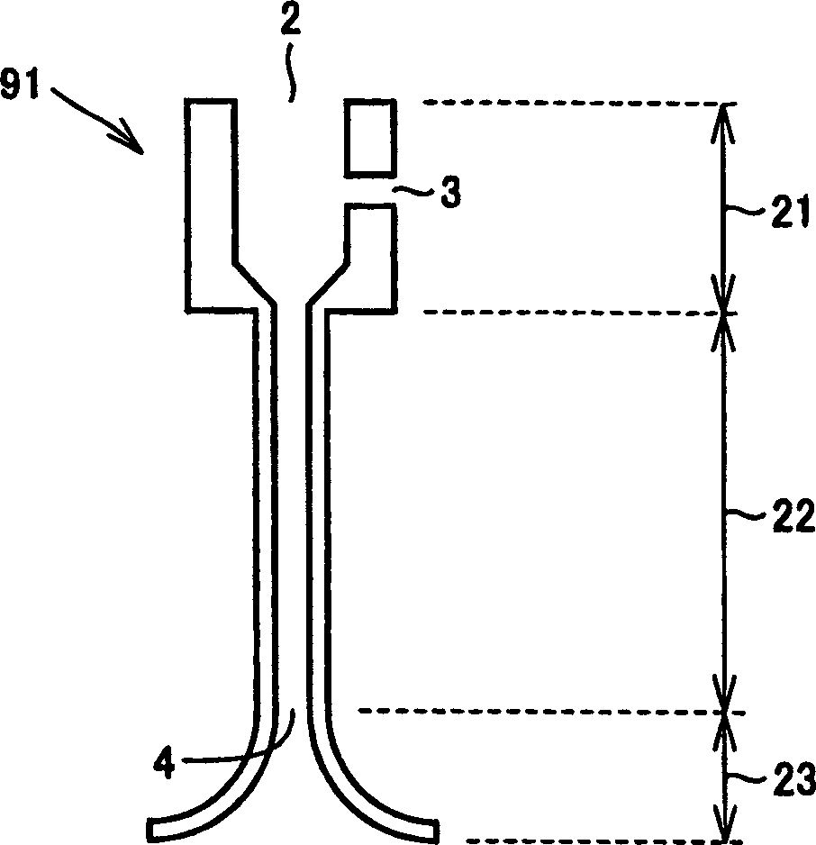
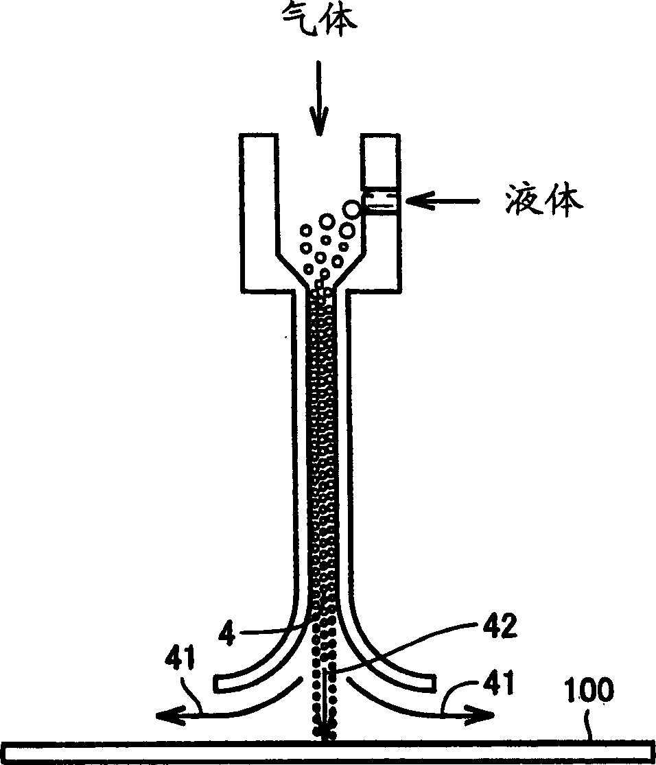
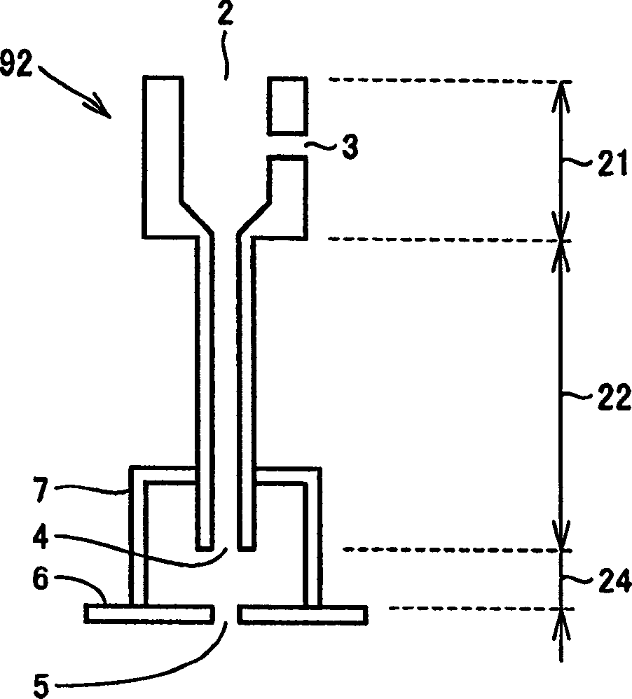
[0038] Refer below Figure 5 The cleaning two-fluid nozzle 93 according to Embodiment 3 of the present invention will be described. This two-fluid nozzle 93 for cleaning has a structure in which the gas shield 6 is connected to the two-fluid nozzle 91 for cleaning shown in the first embodiment.

[0039] In the case of the two-fluid nozzle 93 for cleaning, most of the gas is not directly blown to the target due to the double effect of the curved portion 23 described in Embodiment 1 and the effect of the baffle plate described in Embodiment 2. On the cleaning surface, it is discharged from the side surface from the gap 25 between the bent portion 23 and the gas shielding plate 6 . Therefore, adhesion of particles to the surface to be cleaned can be suppressed, and damage to fine patterns caused by the impact of particles can be prevented.

[0040] (implementation form 4)

[0041] Refer below Figure 6 A cleaning device according to Embodiment 4 of the present invention will ...


PUM

PropertyMeasurementUnit
Lengthaaaaaaaaaa

Abstract

A two-fluid cleaning jet nozzle comprises a mixing part mixing two types of externally supplied fluids with each other for preparing a fluid mixture, a straight pipe linearly and tubularly formed along a prescribed accelerating direction toward the surface of a cleaned substance for accelerating the aforementioned fluid mixture received from the mixing part along the aforementioned accelerating direction, and a bent part connected to an outlet of the straight pipe. The bent part has an inner surface communicating with the inner surface of the straight pipe. The inner surface of the bent part defines a convexly bent curved surface to spread outward with respect to a space receiving the fluid mixture injected from the straight pipe.

Description

technical field [0001] The invention relates to a two-fluid nozzle for cleaning and a cleaning device equipped with the nozzle. In particular, it relates to a two-fluid nozzle for cleaning and a cleaning device for removing contaminants adhering to the surfaces of substrates such as semiconductor wafers, liquid crystal substrates, disk substrates, and photomasks. Furthermore, it relates to the manufacturing method of a semiconductor device. Background technique [0002] It is well known that, in general, various contaminants adhere to semiconductor wafers during the semiconductor manufacturing process. For example, when an insulating film and a metal film are formed on a semiconductor wafer by CVD (Chemical Vapor Deposition) or sputtering, particulate contaminants adhere to the surface on which the film is formed. In addition, after patterning by dry etching, corrosion residues (resist residues) and metal contaminants adhere. As a method for removing these pollutants, as ...

Claims


Application Information

Patent Timeline
IPC IPC(8): G02F1/13B01F3/04B01F5/02B05B1/26B05B7/04B08B3/02H01L21/00H01L21/304
CPCB05B1/265B05B7/0416B08B3/02H01L21/67051B01F3/04049B01F5/0268B01F23/2132B01F25/25H01L21/304
Inventor 菅野至
Owner MITSUBISHI ELECTRIC CORP
Why Eureka
Try Eureka