
Circuit element assembling method

A circuit board and connecting board technology, which is applied in the direction of electrical components, electrical components, and electrical components to assemble printed circuits, etc., can solve problems such as increasing production capacity, shortening production process, and uncoordinated production capacity of semi-finished products

Inactive Publication Date: 2003-05-21
WISTRON CORP +1
View PDF0 Cites 1 Cited by
  • Summary
  • Abstract
  • Description
  • Claims
  • Application Information

AI Technical Summary

Problems solved by technology

[0011] The purpose of the present invention is to provide a method for making a coupler board of a circuit board, which is used to reduce BOM and Artwork preparation work before production and shorten working hours, and even shorten the production process, solve the problem of uncoordinated production capacity of semi-finished products, and increase production capacity. production capacity, and can save the production cost of punching machine and steel plate, and simplify the production process

Method used


Image

  • Circuit element assembling method
  • Circuit element assembling method
  • Circuit element assembling method

Examples


Embodiment Construction

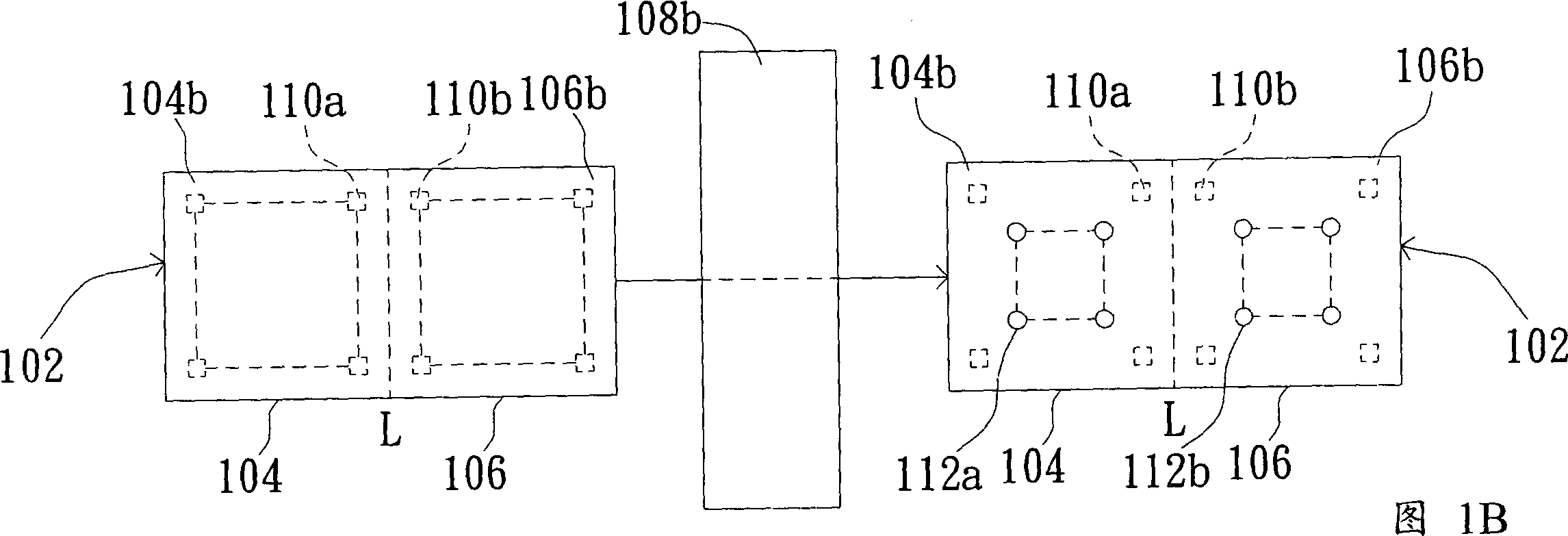
[0018] The present invention specially designs a coupling board punching method for a circuit board. At first, a coupling board with 2N substrates is provided. The value of N is a positive integer. The front side of the coupling board consists of the fronts of N substrates and N connected to the opposite side of a substrate. Then, the coupling board is sent into a punching machine for punching, and several front parts and several reverse parts are formed on the front faces of N substrates and the reverse faces of the other N substrates respectively. Then, the coupling plate is turned over, and the reverse side of the coupling plate is formed by connecting the reverse surfaces of N substrates and the front surfaces of other N substrates. Then, the coupler plate is sent into the punching machine to be punched, and another several front parts are formed on the front faces of the other N substrates, and another several reverse parts are formed on the reverse faces of the N substra...


PUM


Abstract

The present invention provides a method for component insertion on double connected circuit board. A which is provided with 2N base plates, and N is a positive integer. There are N fron surfaces and another N reverse surfaces of the base plates on the front side of double connected circuit board. Deliver it into the insertion machine and form several parts of the front surface and several parts of the reverse surface, and turn over the board. Then deliver board into the insertion machine and form several parts of the front surface on the front side of N base plates and several parts of the reverse surface on the reverse side of N base plates. On the frontal and reverse surface of N base plates, form several frontal parts and reverse parts respectively. Turn-over the couple connection plate.

Description

technical field [0001] The present invention relates to a method for punching circuit boards, in particular to a circuit board that can save a steel plate, a punching machine, a Bill of Material (BOM) and a wall chart (Artwork). Connecting plate punching method. Background technique [0002] Electronic products have become an indispensable part of modern life, especially electronic products with small size and easy to carry, such as notebook computers (Note Book), personal digital assistants (Personal Digital Assistant, PDA), mobile phones ( Cellular Phone) and CD players, etc., are more popular among modern people. Among them, due to the reduction in the size of electronic products, the circuit boards configured in electronic products will also be reduced in size. Therefore, some operators use two punching machines to attach electronic parts to the front and back of the circuit board respectively. on both sides. [0003] Please refer to Figure 1A...

Claims


Application Information

Patent Timeline
Patent Type & Authority Applications(China)
IPC IPC(8): H05K3/30H05K13/04
Inventor 柯斯雄
Owner WISTRON CORP
Learn More