Surface state checking method and circuit board checker

A surface state and inspection device technology, applied in measurement devices, color measurement devices, optical devices, etc., can solve problems such as increased cost, difficulty in detecting leads, and difficulty in realizing optical systems, and achieves the effect of improving accuracy

Inactive Publication Date: 2003-07-23
ORMON CORP
View PDF1 Cites 23 Cited by
  • Summary
  • Abstract
  • Description
  • Claims
  • Application Information

AI Technical Summary

Problems solved by technology

For example, using the above Figure 8 Even if the lead is deflected when observing the upper surface of the lead, if the change of the inclination angle caused by the deflection is very small, it is difficult to detect this small change because it is included in the range that is usually detected by red light. Detects tiny skew on leads
[0012] In this way, when it is desired to observe the inclination state of a steep object in detail or to detect a small change in the inclination angle, it will be difficult to achieve this with the above-mentioned optical system.
[0013] On the other hand, increasing the number of light sources was considered as a method of improving resolution in inclined surface detection, but this would inevitably lead to an increase in cost

Method used


Image

  • Surface state checking method and circuit board checker
  • Surface state checking method and circuit board checker
  • Surface state checking method and circuit board checker

Examples


Embodiment Construction

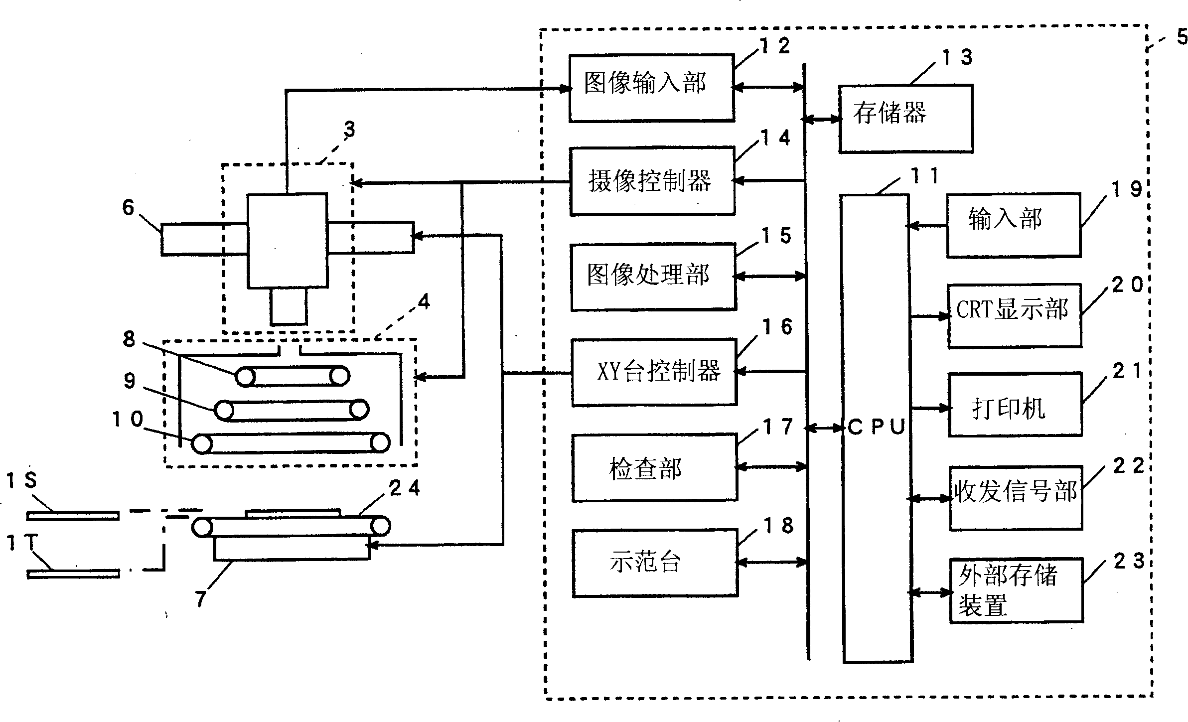
[0066] figure 1 The configuration of a circuit board inspection device according to an embodiment of the present invention is shown.

[0067] This circuit board inspection device is a device that first photographs the circuit board of the inspection object, then processes the obtained image, and then judges whether the solder joint on the circuit board is qualified. It consists of an imaging unit 3, a light projection unit 4, Control processing part 5, X-axis table 6, Y-axis table 7 etc. constitute.

[0068] 1T in the figure is an inspection target circuit board (hereinafter referred to as "inspected circuit board 1T"). 1S is a standard circuit board with good solder joint state and device mounting state, and is used for demonstration before inspection.

[0069] The above-mentioned Y-axis table 7 is equipped with a conveyor belt 24 supporting the circuit boards 1S, 1T, and the conveyor belt 24 is driven by a motor not shown in the figure to make the above-mentioned circuit ...


PUM


Abstract

The invention provides a surface conduction examination method and a substrate examination device, using the optical system which is the same as its prior art to promote the tilting angle resolution, thereby enhancing the examination accuracy. A substrate examination device having a light projecting section 4 consisting of the light sources which emits respectively the R, G, B coloring light and are installed respectively in different azimuth directions with respect to the examination region including soldering portion., extracts 1 or 2 color ingredients which have intensity higher than that of average value. The tilting surfaces adapting to each of light sources 8, 9, 10 are converted respectively into a light and shade monochrome red, green and blue image. Further, the tilting surface at boundary position, which a adapts to light sources 8, 9 is converted into a light and shade image having a color mixed with red and green, whereas the tilting surface at boundary position, which adapts to the light sources 9, 10 is converted into a light and shade image having a color mixed with green and blue.

Description

technical field [0001] The present invention relates to a technique for inspecting the surface state of a predetermined object to be inspected, such as a curved surface of an object with a curved surface such as a solder portion formed on a device-mounted circuit board, and an inclination state of a device lead. Background technique [0002] The applicant has previously developed a device for automatically inspecting solder portions on circuit boards by using the specular reflection characteristics of solder portions and by means of image processing (see Patent Document 1). [0003] Patent Document 1 - Special Publication No. 6-1173 [0004] Figure 8 The configuration and inspection principle of the circuit board inspection device disclosed in the aforementioned Patent Document 1 are shown. This inspection device is a device that generates an image of an inspection object by using three light sources 8, 9, 10 and an imaging device 3 capable of emitting red (R), green (G) a...

Claims


Application Information

Patent Timeline
Patent Type & Authority Applications(China)
IPC IPC(8): G01B11/24G01J3/08G01J3/46G01N21/88G01N21/956
CPCG01N21/95684G01N21/8806
Inventor 村上清藤井良树
Owner ORMON CORP
Why Eureka
Try Eureka