Method for mfg. semiconductor substrate

A semiconductor and substrate technology, applied in the field of semiconductor substrates, can solve the problem that the SiGe layer is not enough for commercial device applications

Inactive Publication Date: 2003-08-13
SHARP KK
View PDF2 Cites 4 Cited by
  • Summary
  • Abstract
  • Description
  • Claims
  • Application Information

AI Technical Summary

Problems solved by technology

However, these investigators reported the relaxation of SiGe layers with a thickness of only 2000 Å-2500 Å and a Ge concentration of less than 22% by molecular weight.
SiGe layers of this thickness are insufficient for commercial device applications

Method used


Image

  • Method for mfg. semiconductor substrate
  • Method for mfg. semiconductor substrate
  • Method for mfg. semiconductor substrate

Examples


Embodiment approach

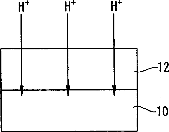
[0045] The method of the present invention can be modified by: growing SiGe layer over 300nm thickness with graded Ge distribution with surface Ge content over 22% + H-II + RTA (to relax SiGe layer stress) + tension table - silicon cap / via . This does not require the deposition of a second SiGe layer.

[0046] Another embodiment of the method of the present invention includes growing the first SiGe layer using either constant or graded Ge distribution + H-II + RTA (to relax the stress of the SiGe layer) + surface Ge content exceeding 22% or constant or graded Ge distribution of the second SiGe layer + tension table - silicon caps / vias. In this embodiment of the inventive method, the thickness of the entire SiGe layer should be 300 nm or higher.


PUM

PropertyMeasurementUnit
thicknessaaaaaaaaaa
thicknessaaaaaaaaaa
thicknessaaaaaaaaaa

Abstract

A method of forming a SiGe layer having a relatively high Ge content includes preparing a silicon substrate; depositing a layer of SiGe to a thickness of between about 100 nm to 500 nm, wherein the Ge content of the SiGe layer is equal to or greater than 22%, by molecular weight; implanting H+ ions into the SiGe layer at a dose of between about 1.1016 cm-2 to 5.1016 cm-2, at an energy of between about 20 keV to 45 keV; thermal annealing the substrate and SiGe layer, to relax the SiGe layer, in an inert atmosphere at a temperature of between about 650° C. to 950° C. for between about 30 seconds and 30 minutes; and depositing a layer of tensile-strained silicon on the relaxed SiGe layer to a thickness of between about 5 mn to 30 nm.

Description

[0001] related application [0002] This application is related to "Method of Forming a Thick Relaxed SiGe Layer on Si," Serial No. 09 / 541,255, filed April 3, 2000, and Serial No. 09 / 54, filed February 13, 2001 783,817 of "Reduced Si 1-x Ge x CMOS Leakage Current Method". technical field [0003] The present invention relates to a method of fabricating a semiconductor substrate, such as a CMOS high-speed integrated circuit, and more particularly to a method of fabricating a semiconductor substrate comprising a step of forming a SiGe layer using hydrogen injection. Background technique [0004] In the application of MOSFET devices with enhanced mobility, thick relaxed Si 1-x Ge x The buffer layer has been used as a practical substrate for thin strained silicon layers to increase the carrier mobility of nMOS devices, Welser et al., Strain dependence of the performance enhancement induced-Si n-MOSFETs, IEDM Conference Proceedings, page 373 ( 1994); Rim et al., Fabrication...

Claims


Application Information

Patent Timeline
Patent Type & Authority Applications(China)
IPC IPC(8): H01L21/205H01L21/20H01L21/265H01L21/322
CPCH01L21/0245H01L21/02694H01L21/02532H01L21/322Y10S438/933H01L21/02381H01L21/20
Inventor 马哲申道格拉斯·詹姆斯·特威滕许胜籘
Owner SHARP KK
Why Eureka
Try Eureka