High quality strain Ge/SiGe super-lattice structure and preparation method thereof

A technology of superlattice and superlattice layer, applied in chemical instruments and methods, single crystal growth, single crystal growth, etc., can solve problems such as high defect density, rough interface/surface, and large thickness

Inactive Publication Date: 2011-08-24
SHANGHAI INST OF CERAMIC CHEM & TECH CHINESE ACAD OF SCI
View PDF0 Cites 39 Cited by
  • Summary
  • Abstract
  • Description
  • Claims
  • Application Information

AI Technical Summary

Problems solved by technology

[0004] The object of the present invention is to provide a high quality strained Ge / Si 1-x Ge x (0.6≤x≤0.7) superlattice structure and its preparation method to overcome the difficulty in preparing high-quality strained Ge / Si in the prior art 1-x Ge x (0.6≤x≤0.7) superlattice, large thickness, high defect density, rough interface / surface, etc.

Method used


Image

  • High quality strain Ge/SiGe super-lattice structure and preparation method thereof
  • High quality strain Ge/SiGe super-lattice structure and preparation method thereof
  • High quality strain Ge/SiGe super-lattice structure and preparation method thereof

Examples


Embodiment 1

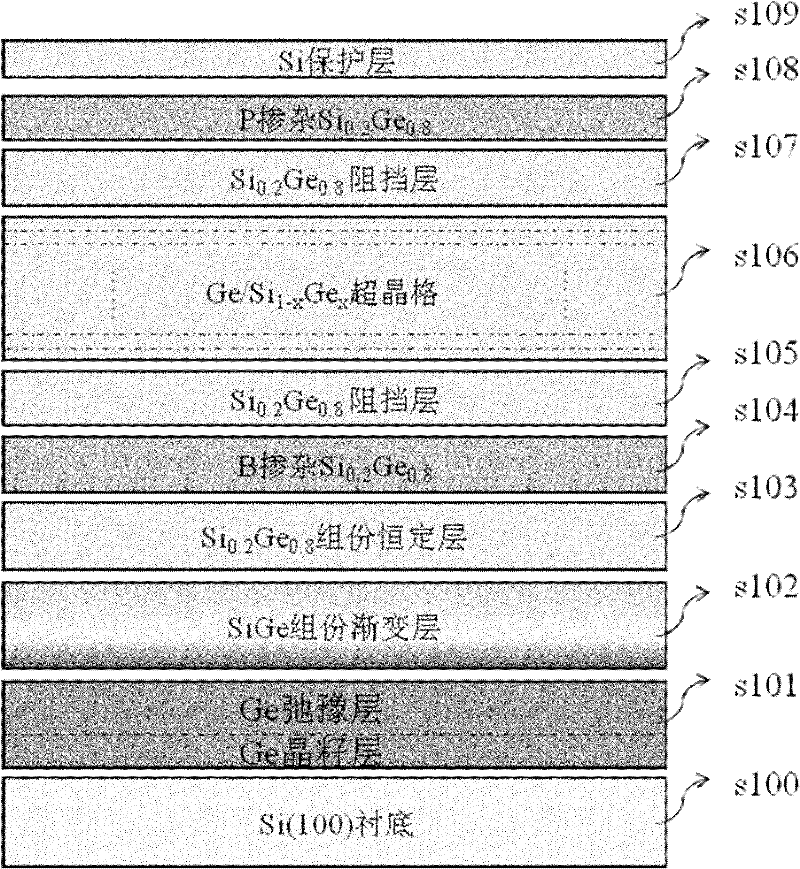
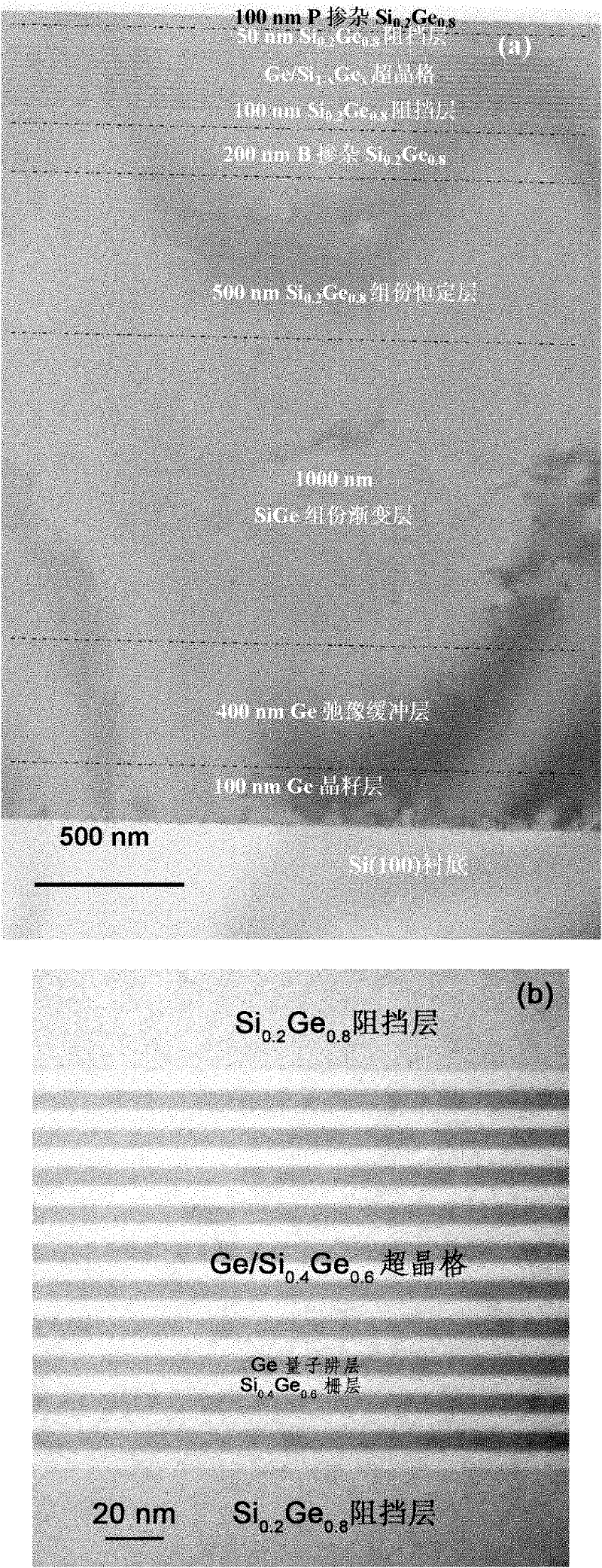
[0060] A high quality Ge / Si 1-x Ge x The preparation process of the superlattice structure is as follows: figure 1 As shown, the preparation of Ge / Si with 10 periods 0.4 Ge 0.6 superlattice, comprising the following steps:

[0061] In step s100, four 4-inch, 6-inch, 8-inch and 12-inch Si (100) wafers are respectively prepared as Si substrates.

[0062] Step s101, growth of Ge relaxation buffer layer: based on 4-inch, 6-inch, 8-inch and 12-inch Si substrates respectively, at 400 ° C with GeH 4 is the gas phase precursor, H 2 For carrier gas, 10% GeH 4 / H 2The gas flow rate is 150sccm, the growth chamber pressure is 100Torr, and a Ge seed layer with a thickness of 100nm is deposited respectively; keep the growth atmosphere unchanged, and then deposit a thickness of 400 nm on the four deposited Ge seed layers at 700°C. The Ge buffer layer of nm is annealed in situ (epitaxial growth chamber) at 850° C. for 10 minutes after completion, and the pressure of the growth chamber...

Embodiment 2

[0079] A 50-period Ge / Si 0.35 Ge 0.65 The preparation of superlattice structure comprises the following steps:

[0080] In step s100, a 4-inch Si wafer is prepared as a Si substrate.

[0081] Step s101, growth of the Ge relaxation buffer layer: on the basis of a 4-inch Si substrate, first at 400 ° C with GeH 4 is the gas phase precursor, H 2 For carrier gas, 10% GeH 4 / H 2 The gas flow rate is 150sccm, the growth chamber pressure is 100Torr, and a Ge seed layer with a thickness of 100nm is deposited respectively; keep the growth atmosphere unchanged, and then deposit Ge with a thickness of 400nm on the deposited Ge seed layer at 700°C. The buffer layer was annealed in situ (in the epitaxial growth chamber) at 850° C. for 10 minutes after completion, and the growth chamber pressure was kept at 100 Torr during annealing to obtain a fully strain-relaxed Ge relaxed buffer layer.

[0082] Step s102, the growth of the composition-graded SiGe buffer layer: on the basis of the r...

Embodiment 3

[0097] A 100-period Ge / Si 0.3 Ge 0.7 The preparation of superlattice structure comprises the following steps:

[0098] In step s100, a 12-inch Si wafer is prepared as a Si substrate.

[0099] Step s101, growth of the Ge relaxation buffer layer: on the basis of a 12-inch Si substrate, first at 400 ° C with GeH 4 is the gas phase precursor, H 2 For carrier gas, 10% GeH 4 / H 2 The gas flow rate is 150sccm, the growth chamber pressure is 100Torr, and a Ge seed layer with a thickness of 100nm is deposited respectively; keep the growth atmosphere unchanged, and then deposit Ge with a thickness of 400nm on the deposited Ge seed layer at 700°C. The buffer layer was annealed in situ (in the epitaxial growth chamber) at 850° C. for 10 minutes after completion, and the growth chamber pressure was kept at 100 Torr during annealing to obtain a fully strain-relaxed Ge relaxation buffer layer.

[0100] Step s102, the growth of the composition-graded SiGe buffer layer: on the basis of t...


PUM

PropertyMeasurementUnit
thicknessaaaaaaaaaa
thicknessaaaaaaaaaa
thicknessaaaaaaaaaa

Abstract

The invention belongs to the technical field of semiconductor materials, and relates to a Ge/Si1-xGex super-lattice structure and preparation thereof. The high quality strain Ge/Si1-xGex super-lattice structure comprises a Si substrate, and a Si0.2Ge0.8 virtual substrate layer, a B-doped Si0.2Ge0.8 epitaxial layer, a Si0.2Ge0.8 blocking layer, a Ge/Si1-xGex super-lattice layer, a P-doped Si0.2Ge0.8 epitaxial layer, a Si0.2Ge0.8 blocking layer and a Si protective layer sequentially and epitaxially grown on the Si substrate, wherein x is more than or equal to 0.6 and less than or equal to 0.7. The epitaxial layers are sequentially grown on the Si substrate by adopting a reduced pressure chemical vapor deposition method; the obtained super-lattice structure has the properties of low dislocation defect density, low thickness and flat interface/surface, and the Ge/Si1-xGex super-lattice is in a strain state; and the super-lattice structure has high quality and is particularly suitable for manufacturing silicon-based laser devices and waveguide modulators.

Description

technical field [0001] The invention belongs to the technical field of semiconductor materials and relates to a high-quality strained Ge / Si 1-x Ge x (0.6≤x≤0.7) superlattice structure and its preparation method. Background technique [0002] With the development of science and technology, human beings have entered into a highly electronic and information society. Information transmission, processing and storage will require unprecedented scale and speed. In the semiconductor industry, semiconductor devices dominated by Si materials have been developed for more than half a century. With the continuous shrinking of the feature size of semiconductor devices, the processing technology of a single transistor has gradually reached the dual limits of physics and technology. How to realize the above-mentioned leap in electronic information technology has become one of the major scientific problems faced in this century. The research on the integration of silicon-based microelec...

Claims


Application Information

Patent Timeline
Patent Type & Authority Applications(China)
IPC IPC(8): C30B29/68C30B25/02
Inventor 刘学超杨建华施尔畏
Owner SHANGHAI INST OF CERAMIC CHEM & TECH CHINESE ACAD OF SCI
Why Eureka
Try Eureka