Method of removing photosensitive resin and residual polymer

A photosensitive resin, polymer technology, applied in photosensitive material processing, electrical components, semiconductor/solid-state device manufacturing, etc., can solve difficult removal, loss of top oxide layer 108, and inability to completely remove sidewall grid polymers And other issues

Inactive Publication Date: 2003-09-10
MACRONIX INT CO LTD
View PDF0 Cites 5 Cited by
  • Summary
  • Abstract
  • Description
  • Claims
  • Application Information

AI Technical Summary

Problems solved by technology

But the disadvantage is: in the process of dry etching, the polymer that makes up the photosensitive resin will be cross-linked (cross-linked) to make the photosensitive resin hard, thus increasing the difficulty of removing the photosensitive resin
However, removing the photosensitive resin 110 by dry etching will make the high molecular polymers constituting the sidewall grid polymer 112 cross-linked and become harder and more difficult to remove.
Therefore, the traditional application of CR solution still cannot completely remove the sidewall grid polymer 112, and some residual polymer 116

Method used


Image

  • Method of removing photosensitive resin and residual polymer
  • Method of removing photosensitive resin and residual polymer
  • Method of removing photosensitive resin and residual polymer

Examples


Embodiment Construction

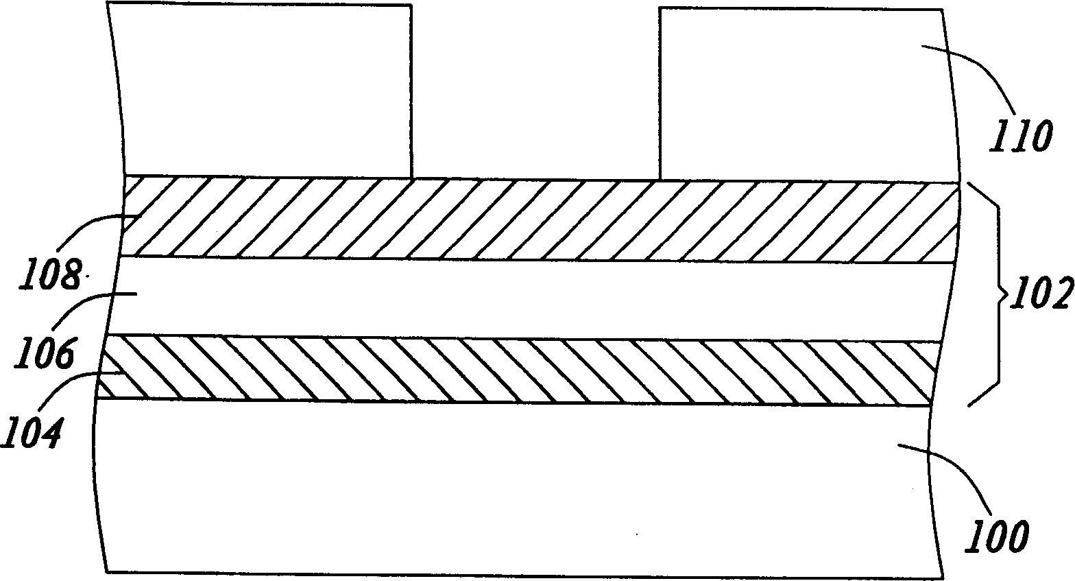
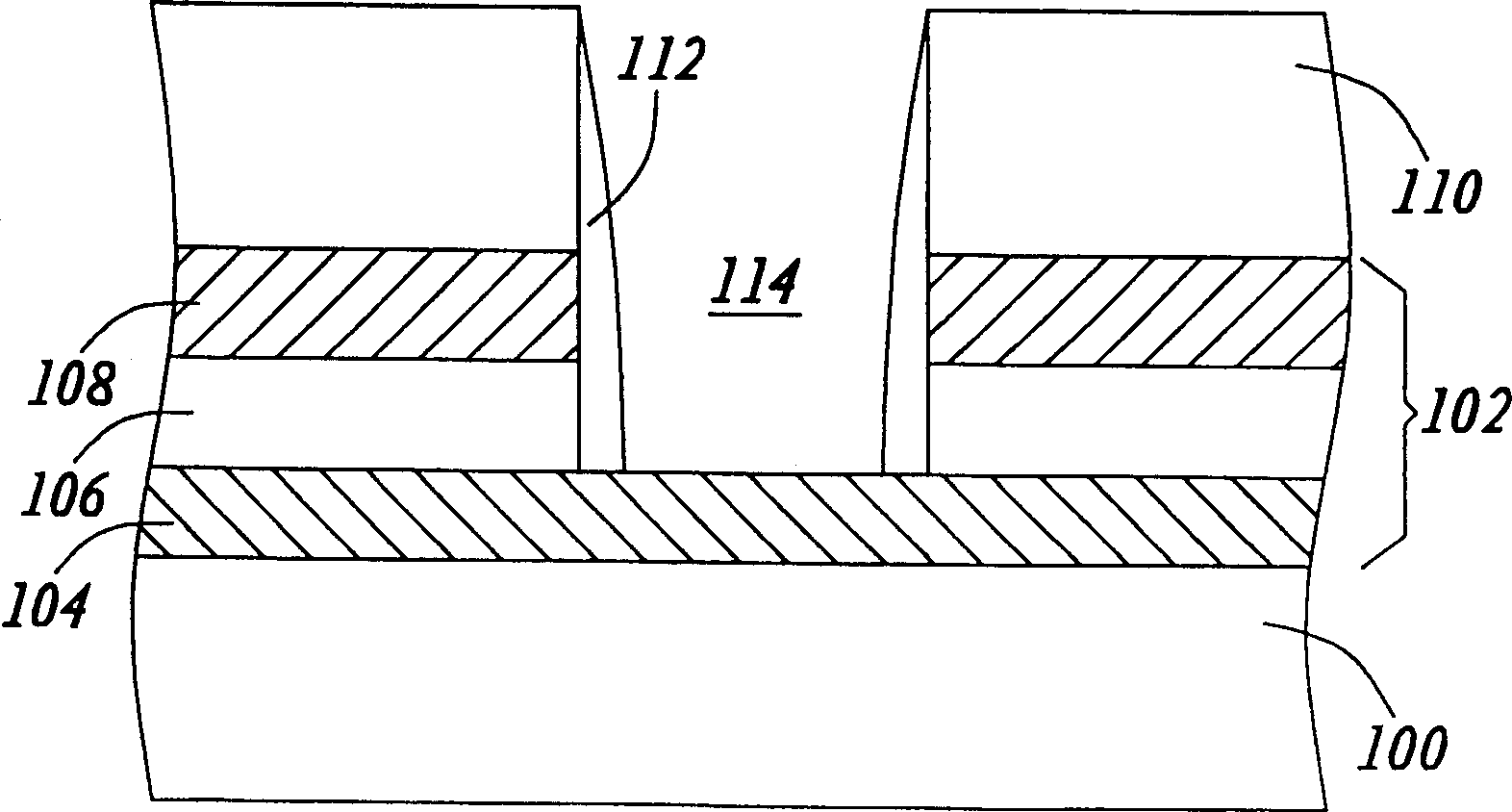
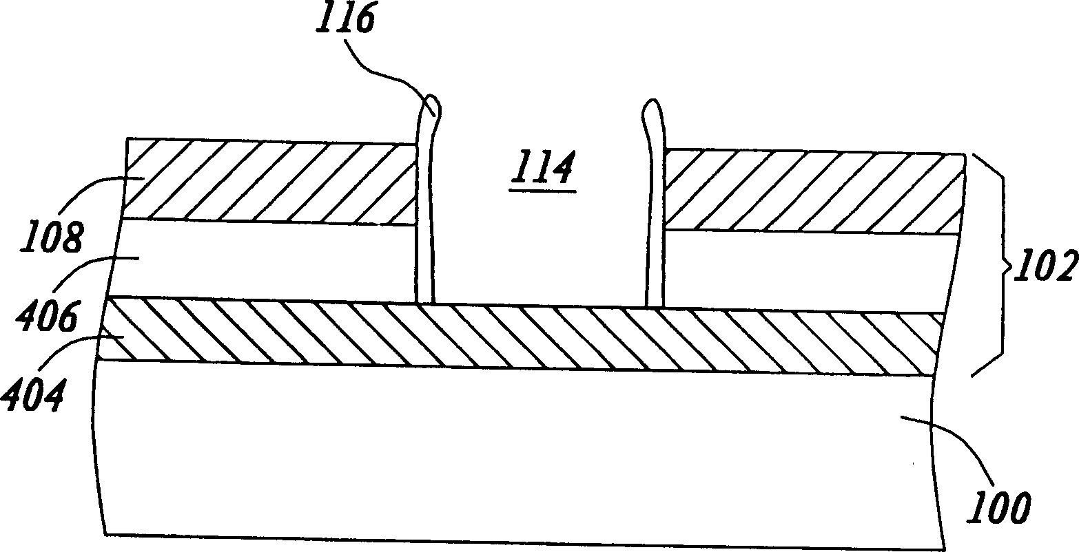
[0019] In this preferred embodiment, a flash memory (flash memory) is taken as an example to illustrate how to remove photo-resist (PR) with the method of the present invention after the formation of a contact hole. And residual polymer (polymer residue) such as sidewall grid polymer (sidewall polymer fence). However, the present invention is not limited to the flash memory, and can also be applied to other semiconductor devices. In addition, in order to express the present invention more clearly, some well-known elements that are irrelevant to the present invention will be omitted from description and not shown in the drawings.

[0020] The etching process for forming the via hole is the same as the conventional method. Please refer to figure 1 and figure 2 . The insulating layer 102 deposited on the substrate 100 is covered with a photosensitive resin, and the photosensitive resin undergoes a photolithography process, such as exposure and development, to form a pattern...


PUM


Abstract

The method of removing photosensitive resin and residual polymer is one wet etching process applying SC1 solution and CR solution successively. The SC1 solution consists of ammonium hydroxide, sulfuric acid and water and is used to remover bar polymer on side walls; and the CR solution consists of sulfuric acid and hydrogen peroxide and is used to remove photosensitive resin. One key point is the application of SC1 solution under low temperature condition to reduce loss of oxide layer. The said wet etching process can remove residual polymer effectively while producting no damage to semiconductor devices.

Description

technical field [0001] The present invention relates to a method for removing photosensitive resin and polymer residue, and in particular to a method for effectively removing photosensitive resin and residual polymer without damaging patterned layers such as insulating Layer (dielectric layer) method. Background technique [0002] In the process of semiconductor manufacturing, the photolithography (Photolithography) process is usually used, such as exposure and development, etc., to transfer the preset pattern on the mask to the photo-resist (PR), and then use the etching process (Etching) The pattern is transferred onto a deposited thin film such as a dielectric layer. After the pattern transfer is completed, the use of the photosensitive resin is also over, and the next important step is to completely remove the photosensitive resin for the subsequent production process. [0003] Recently, dry etching is mostly used in the process of pattern transfer, that is, plasma-etc...

Claims


Application Information

Patent Timeline
IPC IPC(8): G03F7/26
Inventor 吴敬斌李宏文侯东源苏炎辉
Owner MACRONIX INT CO LTD
Why Eureka
Try Eureka