Two-dimensional display device

A flat display and display area technology, applied in static indicators, nonlinear optics, optics, etc., can solve the problems of increasing mass production costs and increasing the complexity of process precision

Inactive Publication Date: 2003-10-29
GIANTPLUS TECH
View PDF0 Cites 9 Cited by
  • Summary
  • Abstract
  • Description
  • Claims
  • Application Information

AI Technical Summary

Problems solved by technology

However, if a very thick transparent conductive layer (or metal conductive layer) is used to improve the difference in resistance value, it will not only increase the mass production cost, but also increase the complexity level of the process precision.

Method used


Image

  • Two-dimensional display device
  • Two-dimensional display device
  • Two-dimensional display device

Examples


Embodiment Construction

[0030] In order to further understand the structure, characteristics and purpose of the present invention, the accompanying drawings and preferred specific embodiments are described in detail as follows:

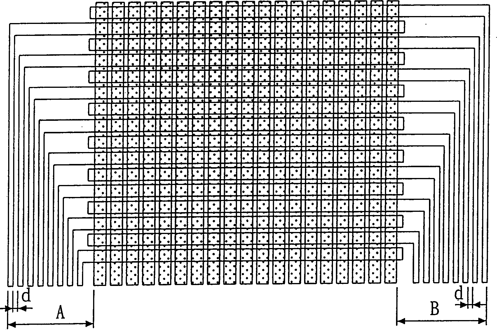
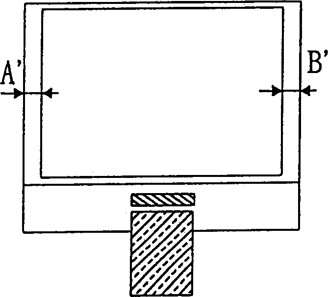
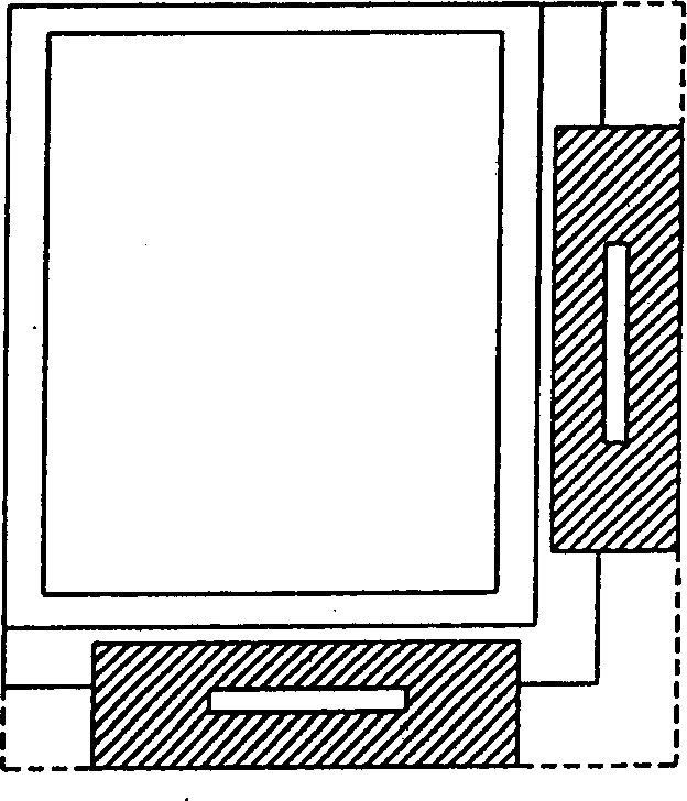
[0031] A preferred embodiment of the present invention, please refer to Figure 4 The three-dimensional exploded schematic diagram of the two-layer panel wiring shown. The display panel of the present invention is mainly composed of a first substrate 1 , a second substrate 2 , and a sealant 3 .

[0032] The materials of the first substrate 1 and the second substrate 2 of the display panel of the present invention are not limited, and may be any commonly used substrates, preferably a glass substrate. The material of the frame glue 3 can be any commonly used frame glue, preferably a frame glue mixed with a conductive substance. In this example, the conductive substance is made of conductive particles 31 (see Figure 6 ).

[0033] The first substrate 1 is the lower substrate...


PUM


Abstract

A two-D display is characterized by that its upper and lower base plates have the leading wire regions at both sides and a display region between two leading wire regions. The part of electrode wiresin the display region and the part of leading wires in the leading wire regions are directly connected. The rest of them are connected with each other via the electric conducting material in peripheral frames, so reducing the area of non-display region.

Description

technical field [0001] The present invention relates to a flat display device, in particular to a wiring of the flat display device. Background technique [0002] Generally, the panel layout of passive small-size liquid crystal display devices uses transparent conductive layers (such as indium tin oxide (ITO)) as leads, and metal lead layout is rarely used, because the use of metal leads will increase mass production costs and the manufacturing process. Accuracy needs to be upgraded. However, due to the limitation of the manufacturing process precision, the layout lead width and lead spacing must maintain a certain width to avoid disconnection and reduce the chance of short circuit. Well-known panel wiring such as figure 1 As shown, the upper substrate and the central display area of ​​the lower substrate of the panel are respectively arranged with vertical and horizontal electrode lines, and each horizontal electrode line is connected to a lead, and there is a distance d ...

Claims


Application Information

Patent Timeline
Patent Type & Authority Applications(China)
IPC IPC(8): G02F1/133G02F1/1343
Inventor 梁伟成张平林昶伸黄文滨
Owner GIANTPLUS TECH
Why Eureka
Try Eureka