This helps you quickly interpret patents by identifying the three key elements:
Problems solved by technology
Method used
Benefits of technology
Problems solved by technology
The problem with the display device of this structure is that it is expensive and it is impossible to reduce the area of the picture frame due to the large area required for bonding the single crystal IC substrate.
Method used
Image
Click on the blue label to locate the original text in one second.
Reading with bidirectional positioning of images and text.
Examples
Embodiment 1
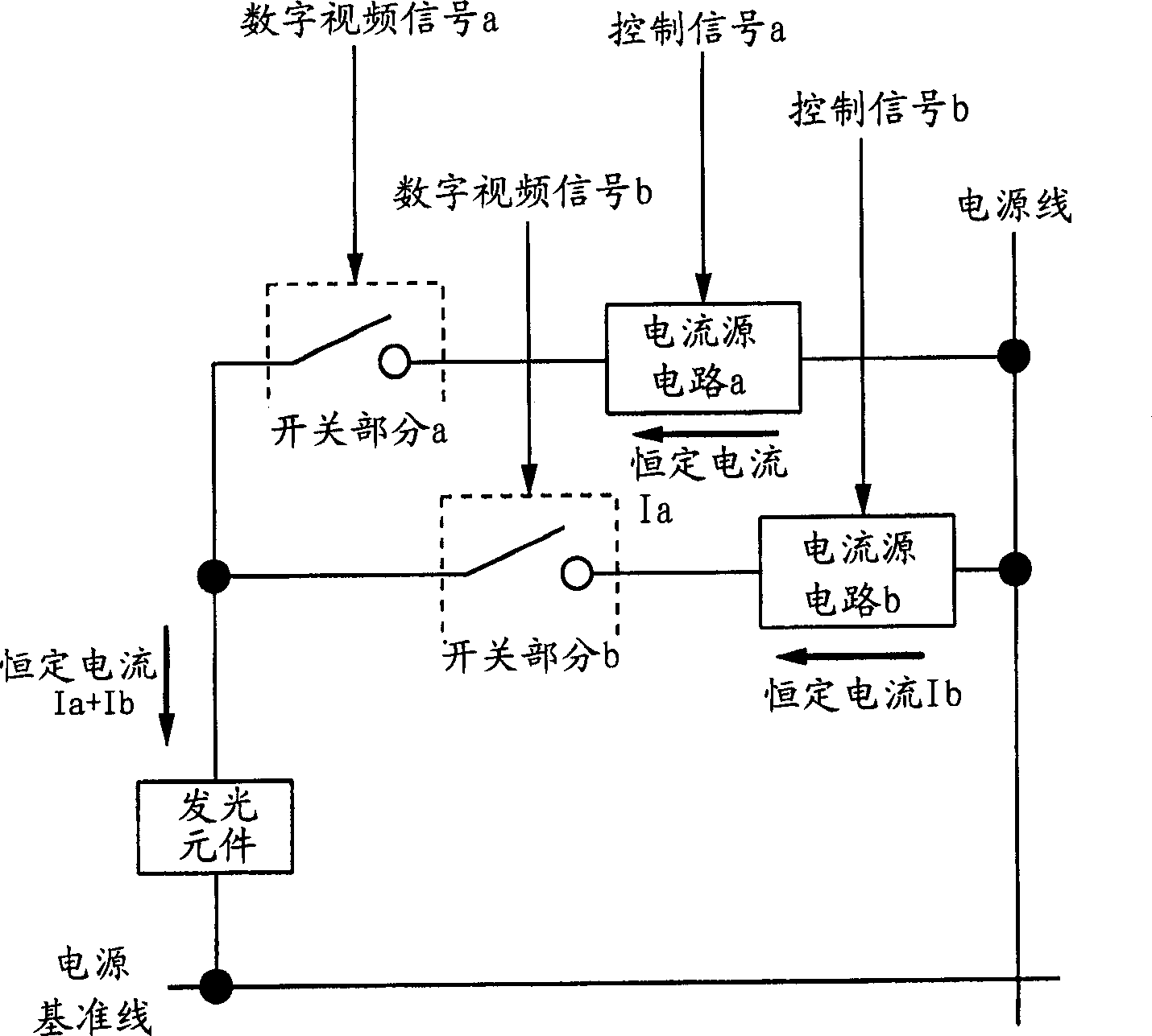
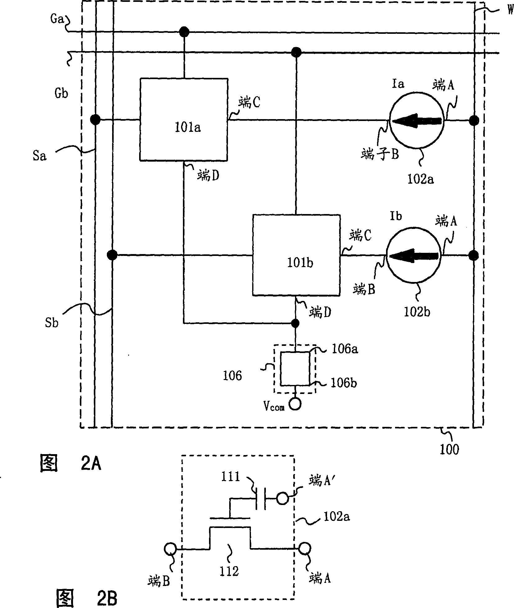
[0111] Next, an embodiment of the present invention is described using FIGS. 2A-C. In this embodiment, a case where there are two pairs within one pixel is described.
[0112] In FIG. 2A, each pixel 100 has switching sections 101a and 101b, current source circuits 102a and 102b, a light emitting element 106, video signal input lines Sa and Sb, scanning lines Ga and Gb, and power supply line W. The switch section 101a and the current source circuit 102a are connected in series to form a pair. The switch section 101b and the current source circuit 102b are connected in series to form a pair. These two pairs are connected in parallel. Also, these two parallel circuits are connected in series with the light emitting element 106 .
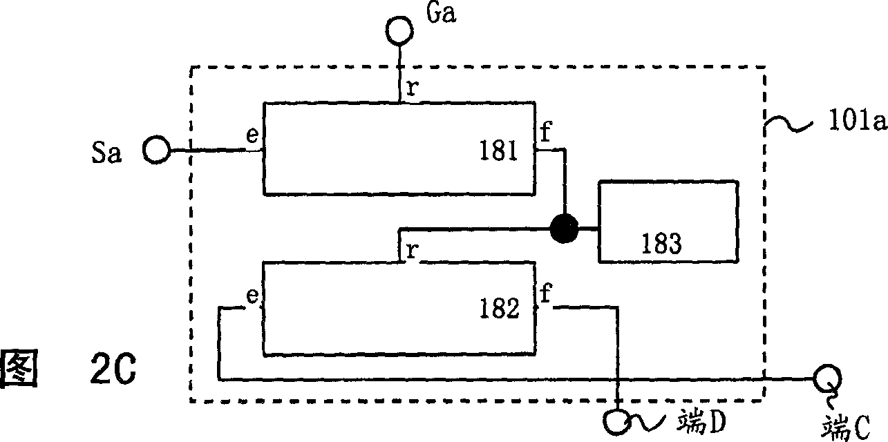
[0113] In the circuit shown in FIGS. 2A-C, two pairs are provided, but the following will focus on the pair of the switch portion 101a and the current source circuit 102a. It is the switch portion 101a and the current source circuit 102a that are des...
Embodiment 2
[0135] The present embodiment represents a specific structural example of a plurality of switching sections of a pixel and a switching section of each pair of current source circuit pairs in the display device of the present invention. Also, the operation of a pixel having a switching portion will be described.
[0136] Such as image 3 Shown is a structural example of the switch section. The switch section 101 has: a selection transistor 301 , a drive transistor 302 , a delete transistor 304 , and a holding capacitor 303 . Furthermore, it is possible to omit the hold capacitor 303 by using the gate capacitance of the drive transistor 302 or the like. The transistors constituting the switch section 101 may be single crystal transistors, or polycrystalline transistors, or amorphous transistors. It can also be an SOI transistor. It can be a bipolar transistor. It could also be a transistor using organic materials, such as carbon nanotubes.
[0167] In this embodiment, the structure and operation of the current source circuit that each pixel of the display device of the present invention has will be described in detail.
[0168] A pair of current source circuits among a plurality of pairs of switch sections and current source circuits is viewed, and its structure is described in detail. In this embodiment, five structural examples of current source circuits are cited, but other structural examples of circuits serving as current sources may be more preferable. In addition, transistors constituting the current source circuit may be single crystal transistors, polycrystalline transistors, or amorphous transistors. It can also be an SOI transistor. Can be a bipolar transistor. It may also be a transistor using organic materials, such as carbon nanotubes.
[0169] First, the current source circuit of the first configuration will be described using FIG. 9A. Furthermore, in FIG. 9A, the same reference numerals and sym...
PUM
Abstract
This invention provides a display apparatus in which it is possible to have a light emitting element emitted light with constant luminance without coming under the influence of deterioration over time, and it is possible to realize accurate gray scale express, and yet, it is possible to speed up writing of a signal current to each pixel, and influence of noise of a leak current etc. is suppressed, and a driving method thereof. A plurality of pairs of switch parts and current source circuits are disposed in each pixel. Switching of each of a plurality of the switch parts is controlled by a digital videosignal. When the switch part is turned on, by a current supplied from the current source circuit making a pair with the switch part, the light emitting element emits light. A current which is supplied from one current source circuit to the light emitting element is constant. A value of a current flowing through the light emitting element is comparable to a value of added currents which are supplied to the light emitting element from respective all current source circuits making pairs with the switch parts which are in the conductive states.
Description
technical field [0001] The present invention relates to a display device using a light emitting element and a driving method thereof. More particularly, the present invention relates to an active matrix type display device and a driving method thereof in which a light emitting element is provided for each pixel and a transistor for controlling light emission of the light emitting element is provided. Background technique [0002] Display devices having light emitting elements have been developed over the years. In particular, active matrix type display devices have been developed in which one light emitting element and one transistor for controlling light emission of the light emitting element are provided for each pixel. [0003] In an active matrix type display device, a technique mainly used is to input luminance information into each pixel through a voltagesignal or to input luminance information into each pixel through a current signal. The former is called a voltage...
Claims
Application Information
Patent Timeline
Application Date:The date an application was filed.
Publication Date:The date a patent or application was officially published.
First Publication Date:The earliest publication date of a patent with the same application number.
Issue Date:Publication date of the patent grant document.
PCT Entry Date:The Entry date of PCT National Phase.
Estimated Expiry Date:The statutory expiry date of a patent right according to the Patent Law, and it is the longest term of protection that the patent right can achieve without the termination of the patent right due to other reasons(Term extension factor has been taken into account ).
Invalid Date:Actual expiry date is based on effective date or publication date of legal transaction data of invalid patent.
