Photoelectric element assembly

A technology for optoelectronic components and components, applied in electrical components, electro-solid devices, circuits, etc., can solve the problems of miniaturization of substrates, lack of margin for insulation spacing, and reduction of luminous efficiency of optoelectronic components, and achieves miniaturization, optical efficiency, etc. The effect of superior utilization rate and superior light utilization efficiency

Inactive Publication Date: 2004-01-28
MATSUSHITA ELECTRIC WORKS LTD
View PDF3 Cites 21 Cited by
  • Summary
  • Abstract
  • Description
  • Claims
  • Application Information

AI Technical Summary

Problems solved by technology

[0008] However, in the above-mentioned photoelectric element components shown in FIG. 17(a) and Patent Document 1, a space for a spacer for wire bonding is required on the bottom surface of the case 110 having an inner peripheral surface having a conical cross-section. limited
For example, when the substrate is reduced in size, there is no margin in the insulation interval between the conductive bonding member 107 and the electrode 105, and there is a risk of a short circuit.
In addition, since the bonding pads and the LED chip 108 are arranged on the bottom surface of the case 110, the LED chip 108 is arranged eccentrically, resulting in a problem that the concentrating property of light deteriorates.
[0009] 17(b) and the photoelectric device shown in Patent Document 2, since the bonding wire 209 is long, it becomes an obstacle in the optical path, which causes a decrease in the luminous efficiency of the photoelectric device.
In addition, when the LED chip 208 is sealed with resin in a subsequent process, the longer the lead wire, the more likely it is affected by the expansion and contraction (thermal stress)

Method used


Image

  • Photoelectric element assembly
  • Photoelectric element assembly
  • Photoelectric element assembly

Examples


Embodiment Construction

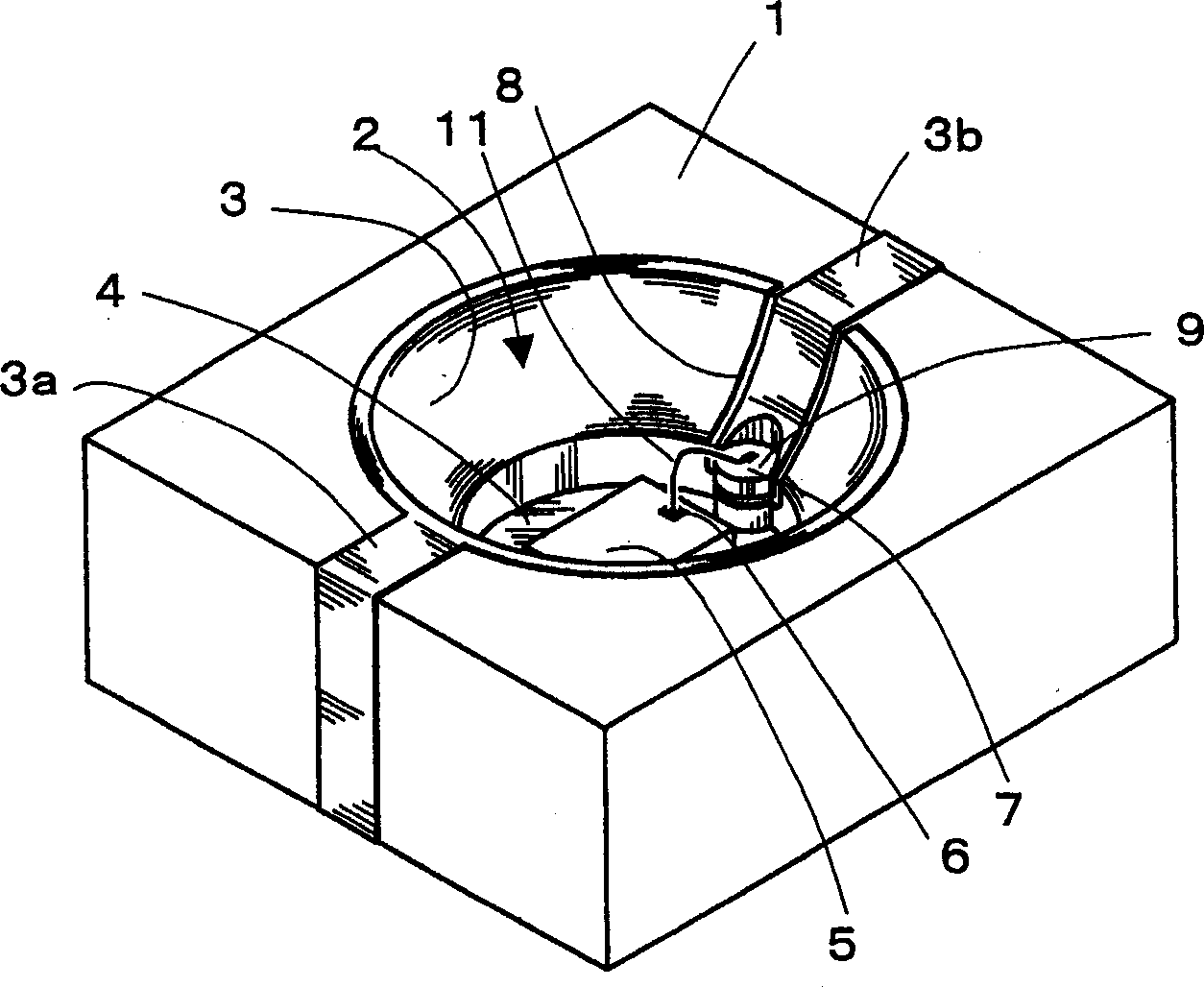
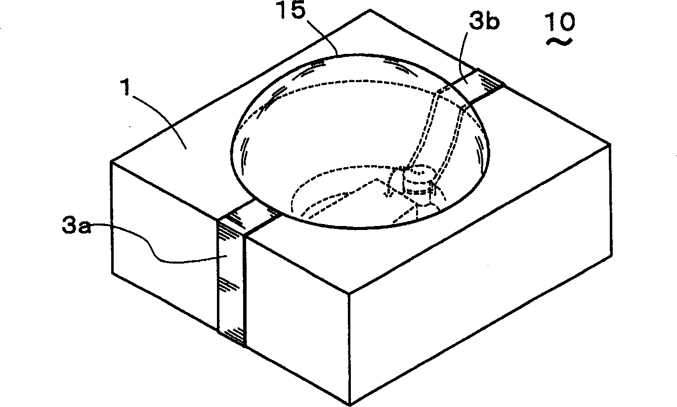
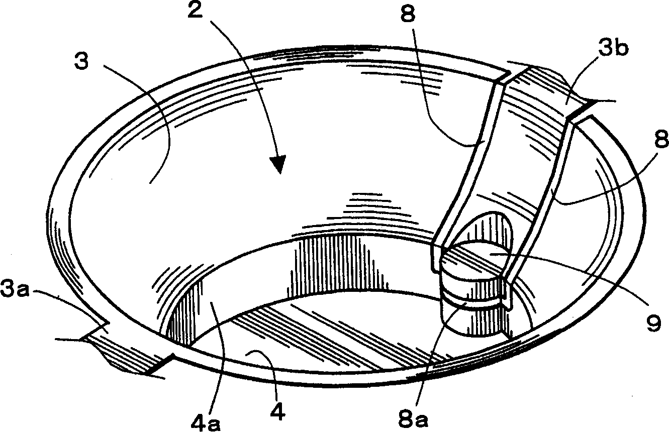
[0069] A photovoltaic element part according to an embodiment of the present invention will be described below with reference to the drawings. figure 1 Indicates the state of the photoelectric element part with the sealing resin layer removed, figure 2 Indicates the appearance of photoelectric element parts. The photoelectric element part 10 is formed by mounting the photoelectric element 5 on the bottom surface 4 of the recess 2 formed in the quadrangular circuit board 1, and is used as a light emitting / receiving device such as an optical connector. The direction of the vertical line at the approximate center of the light emitting / receiving surface of the photoelectric element 5 is defined as an optical axis. A metallized light reflection surface 3 for the photoelectric element 5 to emit / receive light is formed on the back surface including the inclined surface forming the recess 2 .

[0070] The light reflecting surface 3 is provided with an inclined surface made of, for ...


PUM

PropertyMeasurementUnit
Glass transition temperatureaaaaaaaaaa
Elastic coefficientaaaaaaaaaa
Glass transition temperatureaaaaaaaaaa

Abstract

In a photoelectric device-part, a bonding pad is formed without increasing a plane area of a concave part for housing a photoelectric device to implement miniaturization and improvement of the light usability efficiency. A light reflecting surface 3 of nearly a parabola configuration or the like provided for light emission and reception by a photoelectric device 5 is formed on a slanting curved surface constituting a concave part 2 of a circuit substrate 1. A convex portion 9a projecting from the light reflecting surface 3 and a receding concave portion 9b are formed in the middle of the concave part 2. A stage 9 is formed by an upper and bottom surfaces of the convex and concave portions 9a and 9b, respectively. A bonding pad 7 for connecting circuits of the photoelectric device 5 is formed at the stage 9. Since a space for the bonding pad 7 is provided by both concave and convex portions, deformation of the light reflecting surface 3 caused by the receding concave portion 9b and a ratio of intrusion to the bottom surface of the concave part by the projecting convex portion 9a can be both minimized. As a result, the photoelectric device 5 can be mounted without largely lowering light emission efficiency or without decentering the light emitting and receiving center, whereby a photoelectric device-part 10 can be miniaturized.

Description

technical field [0001] The present invention relates to a photoelectric element component in which a photoelectric element is installed in a recess provided on a three-dimensional circuit substrate. Background technique [0002] Conventionally, as a photoelectric element component, a component that performs photoelectric conversion by using a photoelectric element to emit light and receive light is known. For example, the light-emitting device 100 shown in FIG. 17(a) is a photoelectric element part (for example, refer to Patent Document 1): electrodes 105, 106 are formed on the surface of a substrate 101, and a conductive bonding member 107 is placed on the electrode 106. LED (light emitting diode) chip 108 is installed, and the lower side of LED chip 108 is electrically connected to electrode 106, meanwhile, the upper electrode of LED chip 108 is electrically connected to electrode 105 by wire bonding, and the cross section with enlarged aperture from bottom to top is The ...

Claims


Application Information

Patent Timeline
IPC IPC(8): H01L31/0203H01L31/0232H01L33/46H01L33/48H01L33/62
CPCH01L31/0203H01L24/45H01L2924/1815H01L2224/73265H01L2924/12041H01L2224/45144H01L2224/32225H01L33/62H01L33/486H01L2924/30107H01L2224/48091H01L2224/48465H01L2924/01078H01L2224/48227H01L33/46H01L31/0232H01L2924/01079H01L31/02325H01L2924/12042H01L2924/12043H01L2924/14H01L2924/15158H01L2924/181H01L2924/00014H01L2924/00
Inventor 木田忍立田淳吉田浩之桝井幹生
Owner MATSUSHITA ELECTRIC WORKS LTD
Why Eureka
Try Eureka