Method for designing semiconductor device

A semiconductor and device technology, applied in the field of designing semiconductor devices, can solve problems such as design restrictions on via holes and upper layer wiring, reduced design freedom, and reduced degrees of freedom

Inactive Publication Date: 2004-05-05
NEC ELECTRONICS CORP
View PDF1 Cites 2 Cited by
  • Summary
  • Abstract
  • Description
  • Claims
  • Application Information

AI Technical Summary

Problems solved by technology

However, this leads to limitations in the design of via holes and upper layer wiring in one semiconductor device
Therefore, there arises a problem that the degree of freedom of design is reduced
In particular, in recent years, if the improvement of high integration, high performance, and low-voltage operation of semiconductor devices is adopted to reduce wiring width, increase wiring density, improve multilayer wiring, a...

Method used


Image

  • Method for designing semiconductor device
  • Method for designing semiconductor device
  • Method for designing semiconductor device

Examples


Embodiment Construction

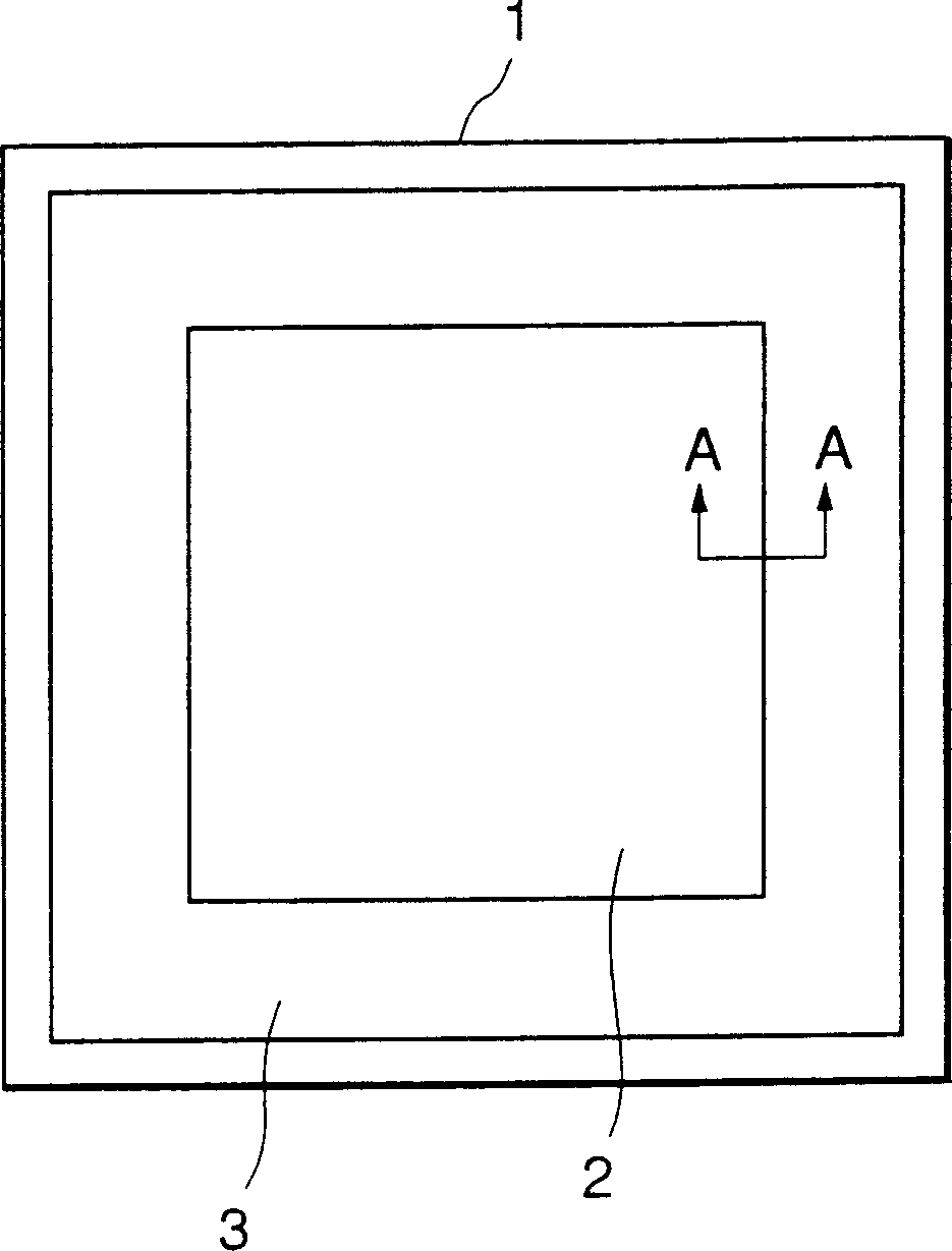
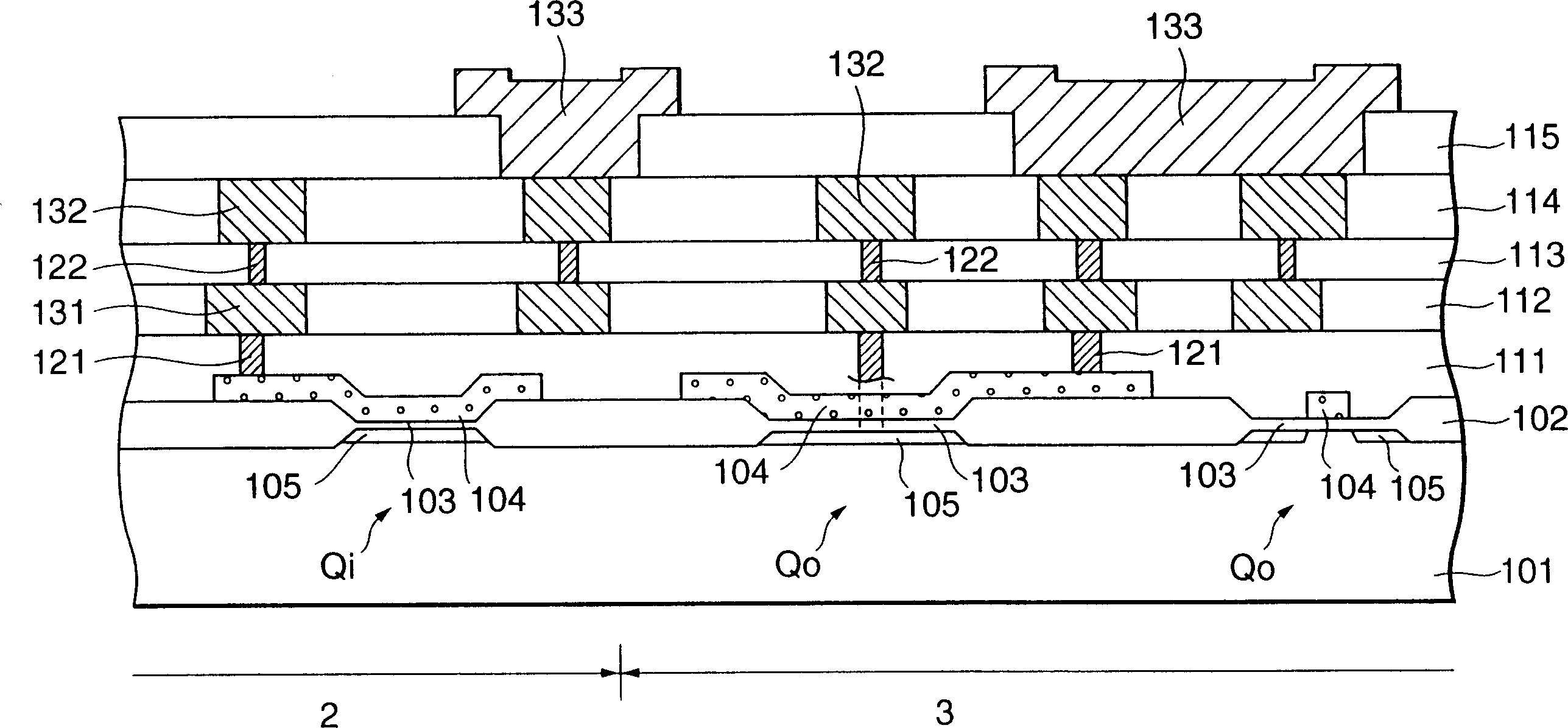
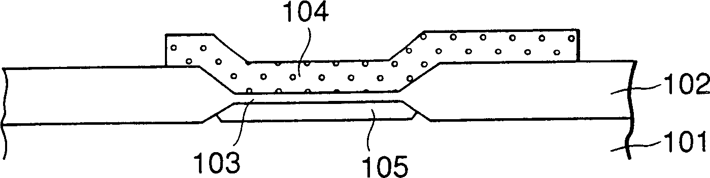
[0031] figure 1 It is a plan view diagrammatically illustrating an example structure of an embodiment of a chip in which the present invention is applied to a semiconductor device including a MOS transistor as an element. In this figure, an internal circuit 2 in which a plurality of tiny minute MOS transistors having a small gate size and constituting memory circuits, logic circuits, etc. are formed is disposed in the central area of ​​the chip. Further, a peripheral circuit 3 in which MOS transistors having a large gate size and constituting an I / O circuit and the like are formed is disposed in a peripheral region on the chip 1 . Then, as described below, necessary circuit connections are made for the MOS transistors of the internal circuit 2 and the peripheral circuit 3 through the upper layer wiring having a layer structure. Now, peripheral circuits are also called I / O elements, or in some cases I / O buffers, and their mounting methods are not limited to figure 1 Periphe...


PUM

PropertyMeasurementUnit
Thicknessaaaaaaaaaa

Abstract

In a mixed-loaded type semiconductor device including a plurality of MOS transistors having gate insulating films different in thickness, the antenna standard for the MOS transistor having the gate insulating film with a thickness equal to or smaller than a predetermined thickness is relaxed compared with that for the MOS transistor having the gate insulating film with a thickness larger than the predetermined thickness. In particular, the antenna standard for the MOS transistor having the gate insulating film with a thickness equal to or smaller than 2.6 nm allowing the tunneling of the electric charges to occur is relaxed compared with that for the MOS transistor having the gate insulating film with a thickness larger than 2.6 nm.

Description

technical field [0001] The present invention relates to a method of designing a semiconductor device including semiconductor elements each having a gate insulating film. In particular, the present invention relates to a method of designing a semiconductor device in which a plurality of semiconductor elements having different gate insulating films are formed integrally with each other on the same substrate. Background technique [0002] In semiconductor elements each having a gate insulating film, such as MOS transistors, problems arise due to degradation of reliability of the gate insulating film, degradation of characteristics of the gate insulating film, or breakdown of the gate insulating film during the manufacture of these elements. For example, in a semiconductor device including a MOS transistor as a semiconductor element, a gate insulating film made of a silicon oxide film or the like is formed on a semiconductor substrate while polysilicon, aluminum or the like Aft...

Claims


Application Information

Patent Timeline
IPC IPC(8): H01L27/04G06F17/50H01L21/3065H01L21/336H01L21/66H01L21/70H01L21/82H01L21/822H01L21/8234H01L21/8238H01L23/544H01L27/088
CPCH01L21/823871H01L21/823857H01L2924/0002H01L2924/00H01L21/3065
Inventor 民田浩靖
Owner NEC ELECTRONICS CORP
Why Eureka
Try Eureka