
Structure of mask ROM and method for manufacturing the same

A technology of read-only memory and manufacturing method, which is applied in semiconductor/solid-state device manufacturing, electric solid-state devices, semiconductor devices, etc., and can solve problems such as misalignment of coding masks, deviation of critical dimensions, easy diffusion of boron ions, etc., and achieve reduction Production cost and the effect of improving the production process margin

Inactive Publication Date: 2004-06-02
MACRONIX INT CO LTD
View PDF0 Cites 2 Cited by
  • Summary
  • Abstract
  • Description
  • Claims
  • Application Information

AI Technical Summary

Problems solved by technology

However, boron ions implanted in the channel region are easy to diffuse into the buried bit lines on both sides
In addition, if the code mask used in the code implantation process has misalignment or critical dimension deviation, the code ions originally planned to be implanted in the channel area will also diffuse into the buried bit line.
The above two situations will cause the ion concentration in the buried bit line to change, so that the current of the buried bit line will be insufficient.

Method used


Image

  • Structure of mask ROM and method for manufacturing the same
  • Structure of mask ROM and method for manufacturing the same
  • Structure of mask ROM and method for manufacturing the same

Examples


Embodiment Construction

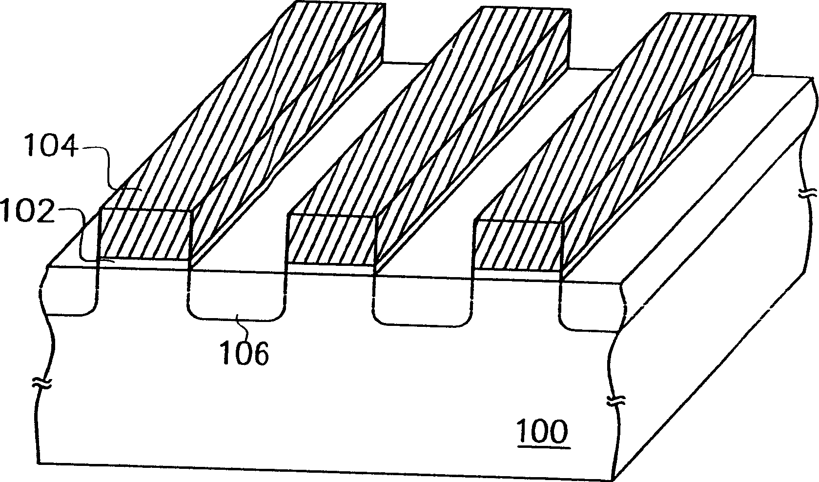
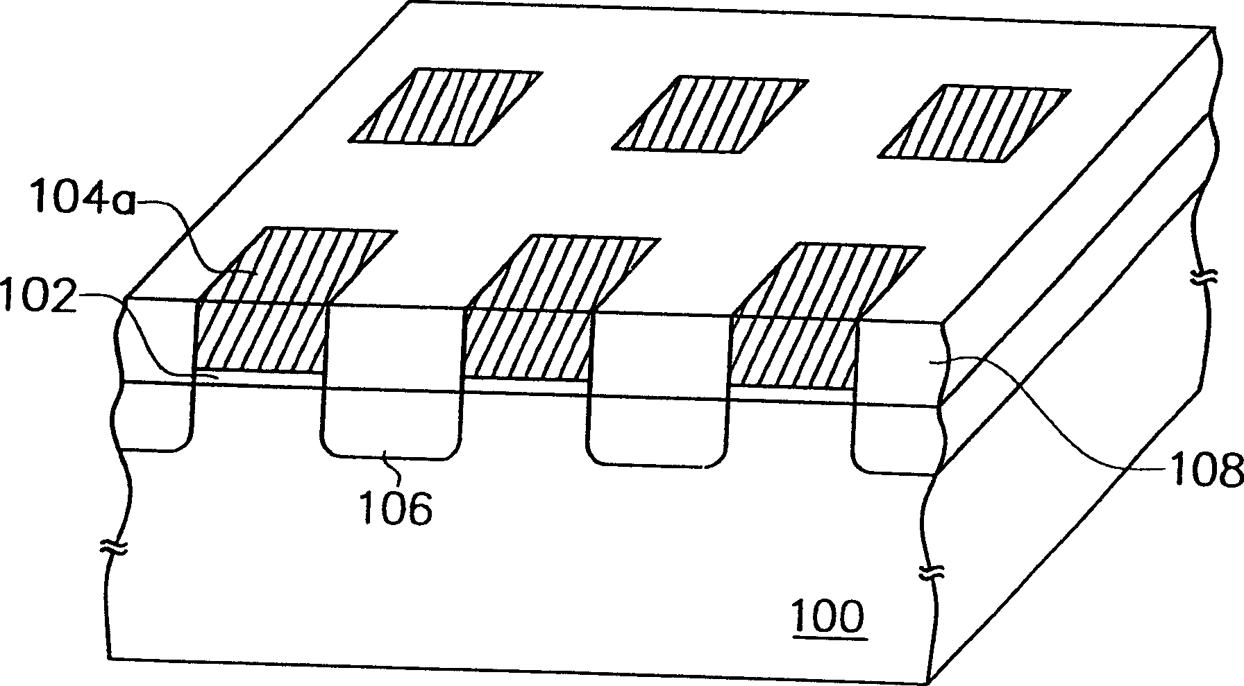
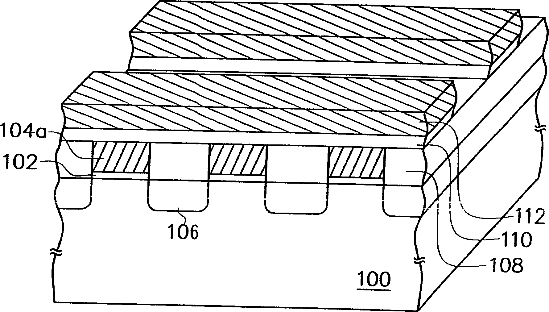
[0022] Figure 1A to Figure 1D As shown, it is a three-dimensional schematic diagram of the manufacturing process of the mask ROM according to a preferred embodiment of the present invention.

[0023] Please refer to Figure 1A , first provide a substrate 100 . Next, a gate dielectric layer 102 and a strip-shaped conductive structure 104 are formed on the substrate 100 . Wherein, the method for forming the gate dielectric layer 102 and the elongated conductive structure 104 is, for example, to firstly use a thermal oxidation method to form a thin oxide layer (not shown) on the surface of the substrate 100, and then form a thin oxide layer on the thin oxide layer. a conductive layer (not shown). Next, the conductive layer is patterned to form strip-shaped conductive structures 104 . Then, the thin oxide layer not covered by the elongated conductive structure 104 is removed to form the gate dielectric layer 102 . In this embodiment, the material of the elongated conductive l...


PUM


Abstract

The invention discloses a screen type read-only memory and and method of manufacture, wherein the arrangement comprises a substrate, a plurality of grid electrodes arranged on the upper portion of part of the substrates, a grid dielectric layer arranged between the substrate and the grid electrode, a plurality of flush type bit lines arranged in the substrate on the two sides of the grid electrodes, an insulating layer arranged between the top of the flush type bit line and the grid electrode, a plurality of word line, each of which is arranged in the same row of grid electrode and insulation layer in the direction perpendicular to the flush type bit line, and encoding layer arranged between the word line and the grid electrode.

Description

technical field [0001] The present invention relates to a memory structure and its manufacturing method, and in particular to a Mask ROM structure and its manufacturing method. Background technique [0002] The structure of a general mask ROM includes several bit lines (Bit Line, BL) and several polysilicon word lines (Word Line, WL) straddling the bit lines. The area below the word line and between two adjacent bit lines is the channel area of ​​the memory cell. For some mask ROMs, the programming method utilizes whether ions are implanted in the channel to store data "0" or "1". The manufacturing process of implanting ions in specific channel regions is also called code implantation manufacturing process. [0003] Usually, the code implantation process of the mask read-only memory first uses a photomask to pattern the photoresist layer formed on the substrate to expose the channel area to be coded. Then, an ion implantation process is performed with the patterned photor...

Claims


Application Information

Patent Timeline
IPC IPC(8): H01L21/8246H01L27/112
Inventor 张庆裕
Owner MACRONIX INT CO LTD
Learn More