Light emitting device

A light-emitting device and light-emitting diode technology, applied in the field of light-emitting devices, provided with circuit substrates, can solve the problems of increased cost of electronic devices and the like

Inactive Publication Date: 2004-06-02
CITIZEN ELECTRONICS CO LTD
View PDF0 Cites 5 Cited by
  • Summary
  • Abstract
  • Description
  • Claims
  • Application Information

AI Technical Summary

Problems solved by technology

In contrast, printing substrates made of metal would increase the cost of electronic devices

Method used


Image

  • Light emitting device
  • Light emitting device
  • Light emitting device

Examples


no. 1 example

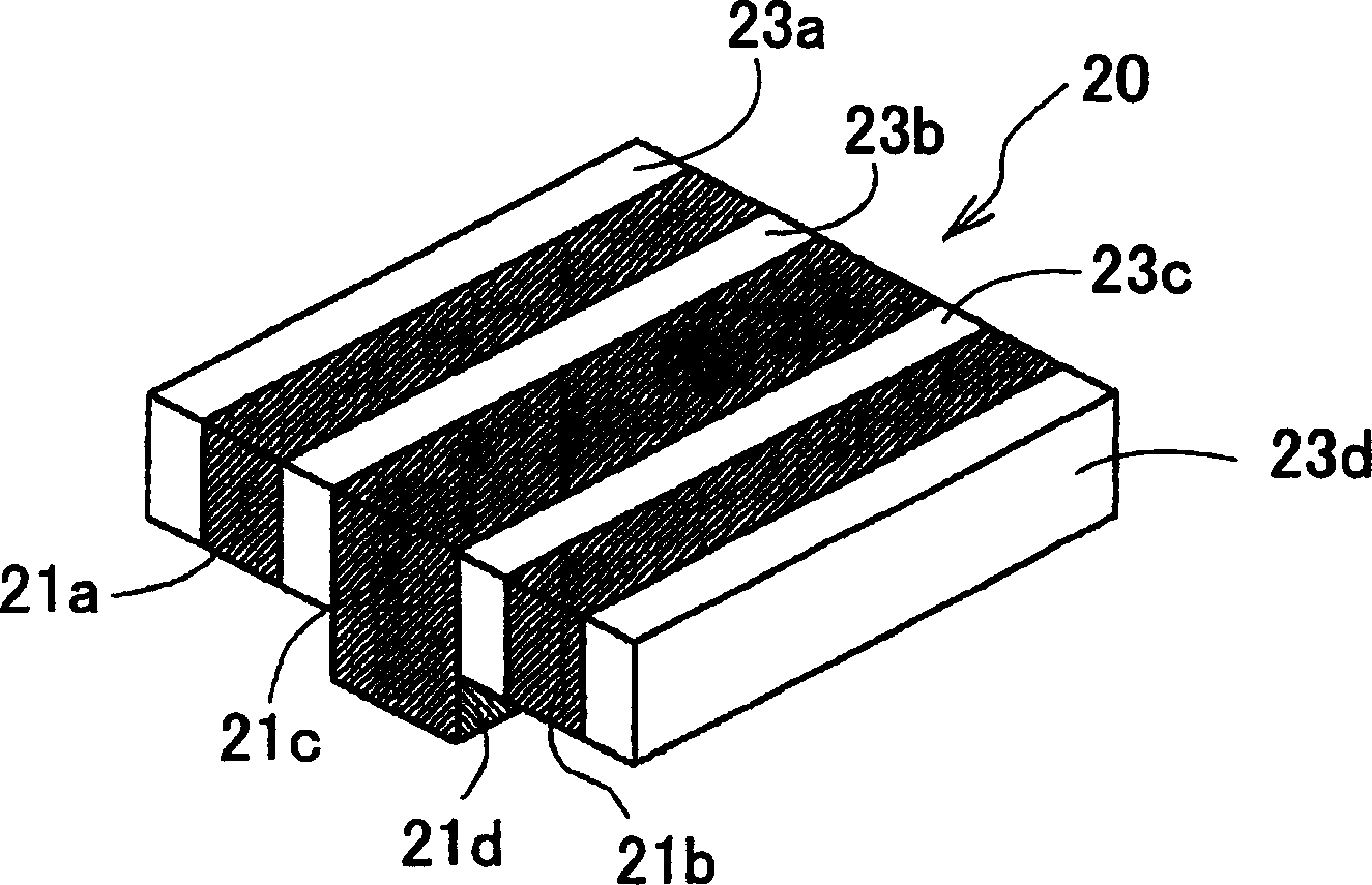
[0033] Figure 10 It is a perspective view of a conductive component assembly and a circuit substrate assembly, illustrating the steps of manufacturing a plurality of light emitting devices according to the first embodiment of the present invention;

[0034] Figure 11 It is an assembly perspective view of a conductive component assembly and a circuit assembly, illustrating the steps of manufacturing a plurality of light emitting devices according to the first embodiment of the present invention;

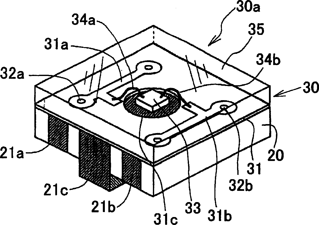
[0035] Figure 12 A perspective view for explaining LED mounting steps for manufacturing a plurality of light emitting devices according to the first embodiment of the present invention;

[0036] Figure 13 A perspective view for explaining a wire connection step for manufacturing a plurality of light emitting devices according to the first embodiment of the present invention;

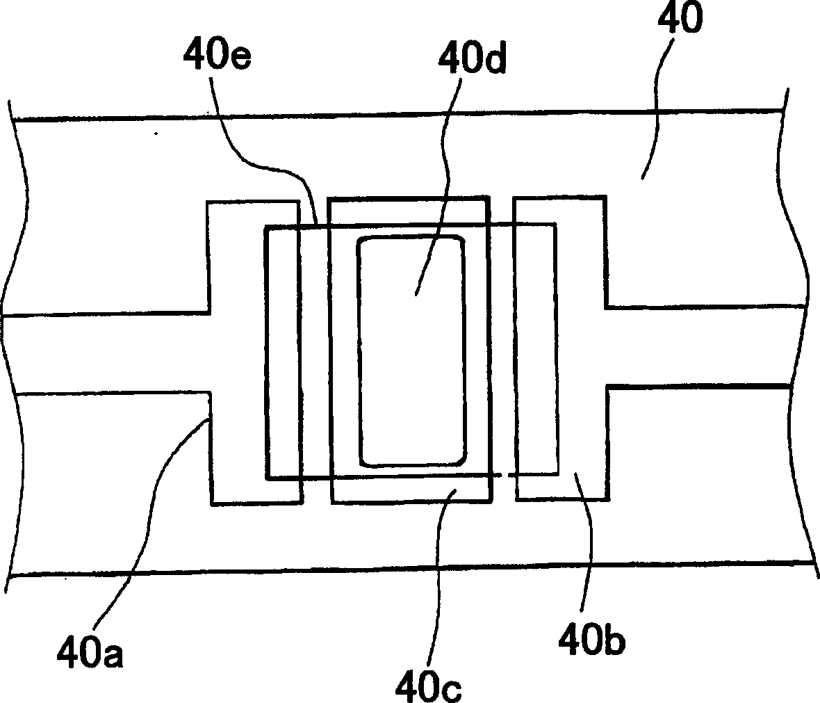
[0037] Figure 14 A perspective view illustrating a packaging step for manufacturing a plurality of ...


PUM


Abstract

A light emitting device has a plurality of conductive members with good heat conductivity provided in a base member, the conductive members are isolated by insulating members provided between the conductive members. A light emitting element device is mounted on the base member. An light emitting diode is provided in the light emitting device and mounted on conductive member. A projection is outwardly projected from the heat conductive member for cooling the LED.

Description

Background of the invention [0001] The present invention relates to light emitting devices using light emitting diodes. [0002] Fig. 16 is a perspective view of a conventional light emitting device disclosed in Japanese Patent No. 3,302,203. The light emitting device 1 comprises a substrate 2 made of resin such as epoxy resin, a pair of electrodes 2a and 2b fixed on the upper and lower sides of the substrate 2, an LED 3 mounted on the electrode 2a and connected to the electrode 2b via a wire 4, and The sealing member 5 made of transparent resin is used to seal the LED3. [0003] The light emitting device 1 is mounted on a printed substrate 6, and the electrodes 2a, ab are connected by a pair of conductive patterns 6a, 6b. [0004] The LED 3 emits light 7 when current is supplied to the LED 3 from the patterns 6a, 6b through the electrodes 2a, 2b. [0005] Since the light emitting device is mounted on the printed substrate 6 through the thin electrodes 2a, 2b, the thickness...

Claims


Application Information

Patent Timeline
Patent Type & Authority Applications(China)
IPC IPC(8): F21V29/00H01L33/48H01L33/56H01L33/62H01L33/64
CPCH01L33/647H01L33/486H01L33/641H01L33/642H01L2224/48091F21V29/004F21Y2101/02H01L2224/48227H01L2224/48472F21V29/74F21V29/75F21Y2115/10F21V29/70H01L2924/00014H01L2924/00
Inventor 矶田宽人
Owner CITIZEN ELECTRONICS CO LTD
Why Eureka
Try Eureka