Image forming method and device, manufacture of device, conductive film layout, photoelectric device and electronic machine

A technology for optoelectronic devices and conductive films, which is used in semiconductor/solid-state device manufacturing, conductive pattern formation, and discharge tube/lamp manufacturing. The effect of forming motion, smooth pattern formation, and suppressing failure

Inactive Publication Date: 2004-09-22
SEIKO EPSON CORP
View PDF2 Cites 1 Cited by
  • Summary
  • Abstract
  • Description
  • Claims
  • Application Information

AI Technical Summary

Problems solved by technology

[0005] However, in the technique of disposing a liquid material as a droplet on a substrate, there is a problem that it is difficult to widen the width of the film pattern.
That is, when the volume of one droplet is increased for the purpose of widening the width of the film pattern or the entire amount of liquid material placed on the substrate is increased, liquid accumulation (bulge) occurs, which may cause failures such as open circuit or short circuit.

Method used


Image

  • Image forming method and device, manufacture of device, conductive film layout, photoelectric device and electronic machine
  • Image forming method and device, manufacture of device, conductive film layout, photoelectric device and electronic machine
  • Image forming method and device, manufacture of device, conductive film layout, photoelectric device and electronic machine

Examples


Embodiment Construction

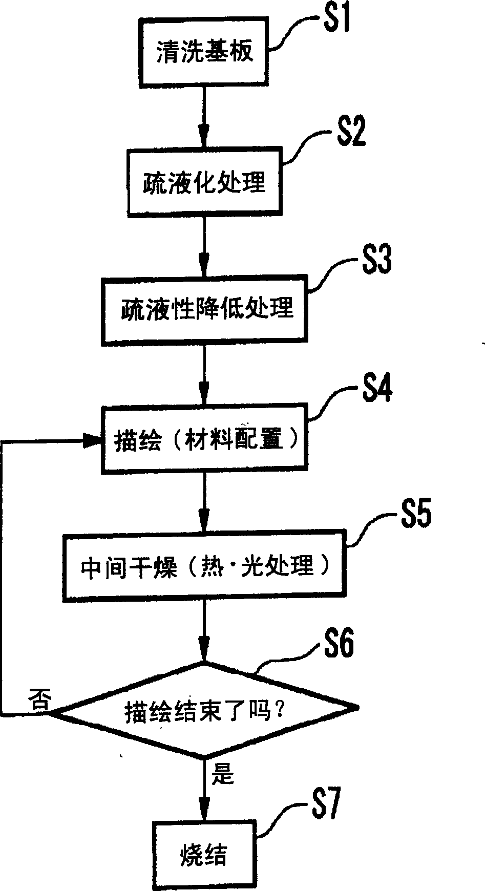
[0046] [Formation method of figure]

[0047]Next, the pattern forming method of the present invention will be described with reference to the drawings. figure 1 It is a flowchart showing an embodiment of the pattern forming method of the present invention.

[0048] Here, in this embodiment mode, a case where a conductive film wiring pattern is formed on a substrate will be described as an example.

[0049] figure 1 Among them, the pattern forming method according to this embodiment includes: a step of cleaning the substrate on which droplets of the liquid material are placed using a predetermined solvent or the like (step S1); a lyophobic treatment step (step S2) constituting a part of the substrate surface treatment step; adjusting A lyophobic reduction treatment step (step S3) that constitutes a part of the surface treatment process to lyophobicize the surface of the substrate after the lyophobic treatment; disposing the wiring including the conductive film on the surface ...


PUM

PropertyMeasurementUnit
particle diameteraaaaaaaaaa
surface tensionaaaaaaaaaa

Abstract

A pattern forming method is provided which discharges droplets of a liquid material on a substrate and forms a film pattern W. The method comprises a first step of forming a central pattern W1 of the film pattern W on the substrate, a second step of forming a first side pattern W2 with respect to the central pattern W1, and a third step of forming a second side pattern W3 with respect to the central part W1.

Description

technical field [0001] The present invention relates to a pattern forming method and a pattern forming device for forming a film pattern by disposing droplets of a liquid material on a substrate, a device manufacturing method, conductive film wiring, a photoelectric device and an electronic machine. Background technique [0002] Conventionally, photolithography is often used as a method of manufacturing devices having fine wiring patterns (film patterns) such as semiconductor integrated circuits, but a method of manufacturing devices using a droplet discharge method is attracting attention. This droplet discharge method has advantages such as less waste of liquid material and easy control of the amount and position of the liquid material disposed on the substrate. Techniques related to the liquid droplet discharge method are disclosed in the following patent documents. [0003] Patent Document 1: Japanese Unexamined Patent Application Publication No. H11-274671 [0004] Pa...

Claims


Application Information

Patent Timeline
Patent Type & Authority Applications(China)
IPC IPC(8): G02F1/1343B05C5/00B05D1/26B05D5/12H01B13/00H01J9/02H01J11/22H01J11/34H01L21/027H01L21/288H01L21/3205H01L21/768H01L51/00H01L51/50H05B33/10H05B33/26H05K3/10H05K3/12
CPCH05K2203/1476H05K3/125H01J2217/49207H01L51/0005H01J9/02H10K71/135H01L21/4867H01L21/6715
Inventor 平井利充长谷井宏宣
Owner SEIKO EPSON CORP
Why Eureka
Try Eureka