Complementary semiconductor and assembling element thereof

A technology of combining components and semiconductors, applied in the direction of transistors, etc., can solve problems such as insufficient space, and achieve the effects of solving insufficient space, improving resolution, and reducing width

Inactive Publication Date: 2004-11-24
AU OPTRONICS CORP
View PDF0 Cites 4 Cited by
  • Summary
  • Abstract
  • Description
  • Claims
  • Application Information

AI Technical Summary

Problems solved by technology

[0010] Therefore, the object of the present invention is to provide a complementary metal oxide semiconductor and its combined components, so as to reduce its layout width, thereby improving resolution and solving the problem of insufficient space

Method used


Image

  • Complementary semiconductor and assembling element thereof
  • Complementary semiconductor and assembling element thereof
  • Complementary semiconductor and assembling element thereof

Examples


no. 1 example

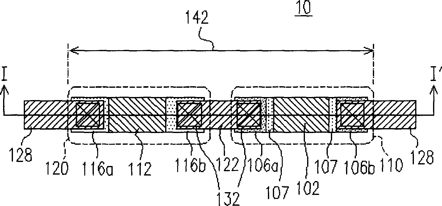
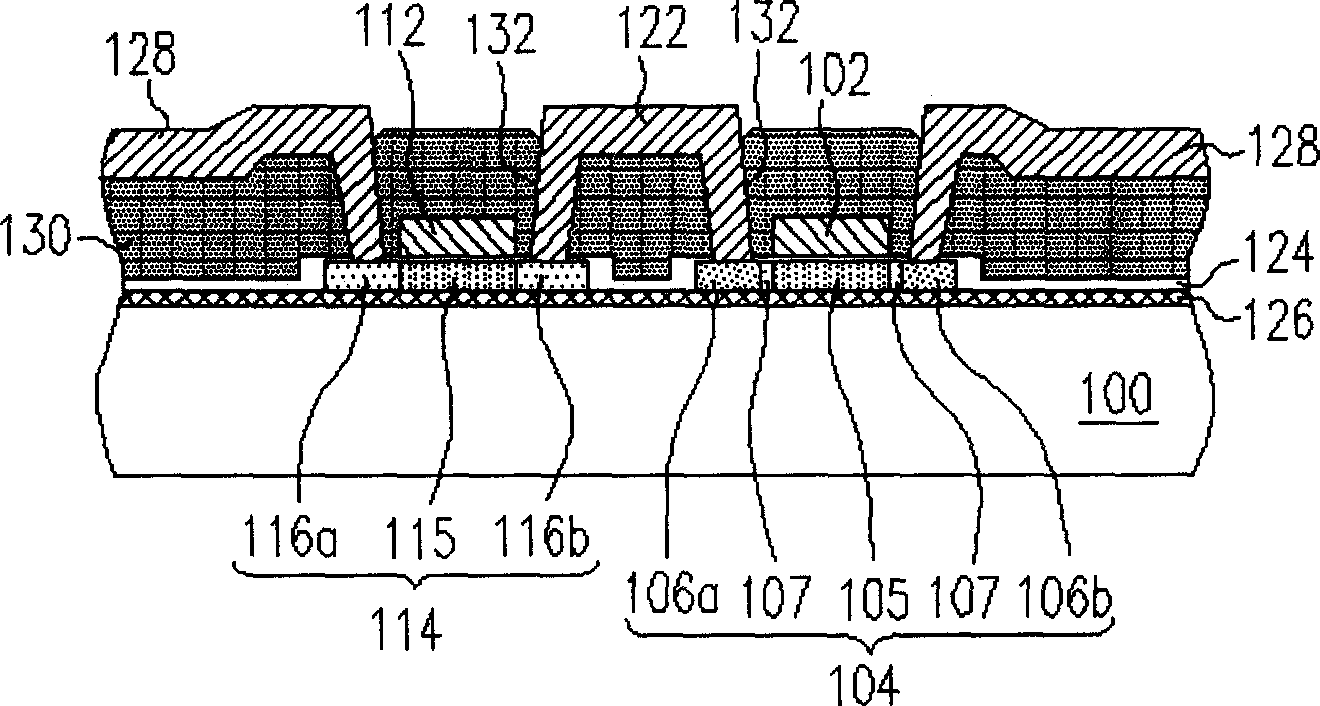
[0046] The present invention can be applied to low temperature polysilicon (low temperature poly-Si, LTPS for short) thin film transistor (thin film transistor, TFT for short), please refer to Figure 2A and Figure 2B .

[0047] Figure 2A is a schematic top view of a complementary metal oxide semiconductor (CMOS) according to a first embodiment of the present invention, and Figure 2B is based on Figure 2A The cross-sectional schematic diagram of the II-II' section.

[0048] Please refer to Figure 2A and Figure 2B , the complementary metal oxide semiconductor 20 of the present invention includes an N-type low-temperature polysilicon thin film transistor 210 and a P-type low-temperature polysilicon thin-film transistor 220 located on a substrate 200, and an interlayer dielectric layer is covered on the low-temperature polysilicon thin-film transistor 210 and 220 (inter-layer dielectrics, ILD for short) 230. In this embodiment, the N-type low-temperature polysilicon ...

no. 2 example

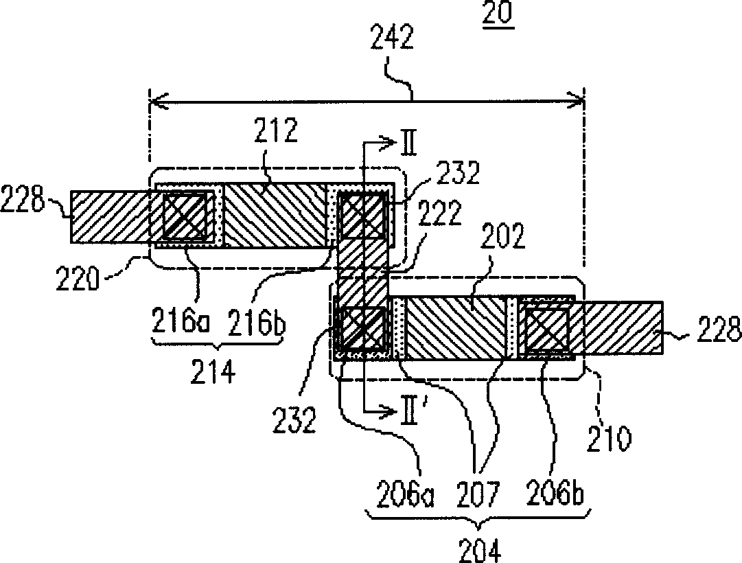
[0054] Any circuit structure composed of at least one P-type thin film transistor and at least one N-type thin film transistor can be laid out by using the present invention, please refer to image 3 .

[0055] image 3 It is a schematic top view of a CMOS composite device according to a second embodiment of the present invention. Please refer to image 3 , the combined element 30 of the present invention includes an N-type low-temperature polysilicon thin film transistor 310 and two P-type low-temperature polysilicon thin film transistors 320 . Although there are only three thin film transistors in this embodiment, it is not limited to the application of the present invention, but only used as an example, so as long as the design is according to the characteristics of the present invention, no matter how many thin film transistors are available.

[0056] Please continue to refer to image 3 , the N-type low-temperature polysilicon thin film transistor 310 of this embodime...


PUM


Abstract

The present invention provides a complementary metal oxide semiconductor, and it is made up by using a first type film transistor and a second type film transistor, and the first type film transistor includes a grid, a channel zone, a first type doped zone and a source doped zone, in which the channel zone, first type doped zone and source doped zone are arranged along a first direction, and the second type film transistor includes a grid, a channel zone, a second type doped zone and a drain doped zone, in which the channel zone, second type doped zone and drain doped zone are also arranged along first direction, and the second type doped zone and first type doped zone are arranged along a second direction, and the second direction is perpendicular to first direction, and the doped zones of all the film transistors are electrically connected by means of a conducting wire, in which the extensive direction of above-mentioned conducting wire is second direction.

Description

technical field [0001] The present invention relates to a low temperature polysilicon (low temperature poly-Si, LTPS for short) thin film transistor (thin film transistor, TFT for short), in particular to a low temperature polysilicon low temperature polysilicon thin film transistor composed of two different types (type) of low temperature polysilicon. A complementary metal oxide semiconductor (CMOS) and its combination components. Background technique [0002] With the development of high technology, video products, especially digital video or image devices have become common products in daily life. In these digital video or image devices, the display is an important component to display relevant information. Users can read information from the display, or further control the operation of the device. [0003] Recently, in thin-film transistor liquid crystal displays, there is a kind of thin-film transistor made by polysilicon technology, whose electron mobility (mobility)...

Claims


Application Information

Patent Timeline
Patent Type & Authority Applications(China)
IPC IPC(8): H01L27/092
Inventor 胡珍仪孙文堂
Owner AU OPTRONICS CORP
Why Eureka
Try Eureka