Manufacturing method of semiconductor device and oxidization method of semiconductor substrate

A manufacturing method and semiconductor technology, applied in semiconductor/solid-state device manufacturing, electrical components, circuits, etc., can solve problems such as not pointing out the oxide film, not describing the conditions of the oxide film, etc.

Inactive Publication Date: 2004-12-01
PS4 LUXCO SARL
View PDF0 Cites 4 Cited by
  • Summary
  • Abstract
  • Description
  • Claims
  • Application Information

AI Technical Summary

Problems solved by technology

However, Reference 4 does not indicate a method of forming an oxide film having a locally different thickness in single oxide film formation, and a change in the thickness of the oxide film within the STI region, and it does not describe the conditions required for oxide film formation, such as HCI oxidation concentration

Method used


Image

  • Manufacturing method of semiconductor device and oxidization method of semiconductor substrate
  • Manufacturing method of semiconductor device and oxidization method of semiconductor substrate
  • Manufacturing method of semiconductor device and oxidization method of semiconductor substrate

Examples


Embodiment Construction

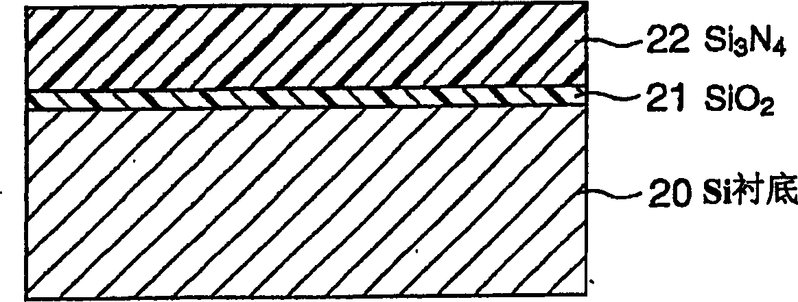
[0039] refer to Figure 1 to Figure 7 , a method for manufacturing a semiconductor device according to an embodiment of the present invention is described step by step. Here, as an example, the manufacture of a DRAM as a semiconductor device will be described. refer to figure 1 , a silicon oxide film 21 and a silicon nitride film 22 are sequentially formed on a silicon substrate 20 by ordinary techniques.

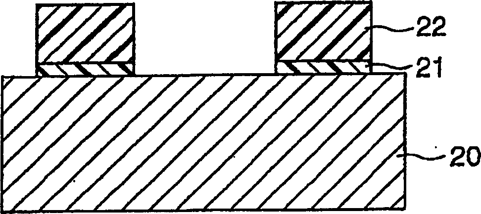
[0040] Next, if figure 2 As shown, after the region where the groove is to be formed is covered by a mask (not shown), the silicon nitride film 22 and the silicon oxide film 21 are selectively etched using photolithography and dry etching techniques, and the silicon substrate Only silicon nitride film 22 and silicon oxide film 21 in the element region remain on substrate 20, and the surface of silicon substrate 20 is divided into an element region and a region for groove formation.

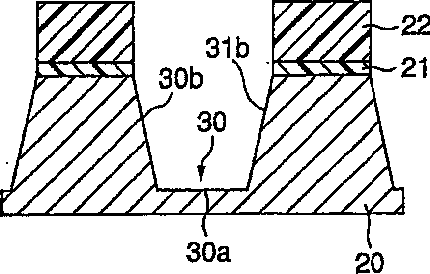
[0041] In this case, as image 3 As shown, the silicon oxide film 21 and the silicon ...


PUM


Abstract

A manufacturing method of a semiconductor device having a trench is provided to form, at a corner portion of the trench, an oxide film which is greater in thickness and smaller in stress than at other portions. When the trench formed in the semiconductor substrate is oxidized, it is oxidized in an oxygen environment containing dichloroethylene at a predetermined weight percent to allow the formation of an oxide film having a greater thickness at the corner portion of the trench than thickness at other portions, whereby the semiconductor device improving dielectric breakdown characteristics can be obtained.

Description

technical field [0001] The present invention relates to a method of manufacturing a semiconductor device including an STI (Shallow Trench Isolation) edge, and more particularly, to a method of oxidizing a trench formed in a semiconductor substrate. Background technique [0002] Hitherto, in semiconductor devices such as DRAMs, STI technology has been used to form an element region surrounded by an insulator-filled trench on one surface of a silicon substrate, and a MOS transistor having source and drain regions is formed in In the component regions, gates, capacitors and wiring layers are then formed in these component regions. When such a semiconductor device is manufactured, the STI region is formed by filling an insulator into the groove formed in the silicon substrate before removing the remaining insulating film in the silicon substrate near the groove, and the gate oxide film and gate formed on the semiconductor substrate adjacent to the trench. The structure of this...

Claims


Application Information

Patent Timeline
Patent Type & Authority Applications(China)
IPC IPC(8): H01L21/76H01L21/316H01L21/762
CPCH01L21/76232
Inventor 久保田大志北村义裕大桥拓夫樱井进神田隆行堀部晋一
Owner PS4 LUXCO SARL
Why Eureka
Try Eureka