Ink jet head method for producing ink-jet head and use
A manufacturing method and technology of an inkjet head, applied in the field of inkjet heads and inkjet recording devices, capable of solving problems such as reduced withstand voltage, prone to insulation breakdown, and electric field concentration
- Summary
- Abstract
- Description
- Claims
- Application Information
AI Technical Summary
Problems solved by technology
Method used
Image
Examples
Embodiment 1
[0125] Composition of Inkjet Head
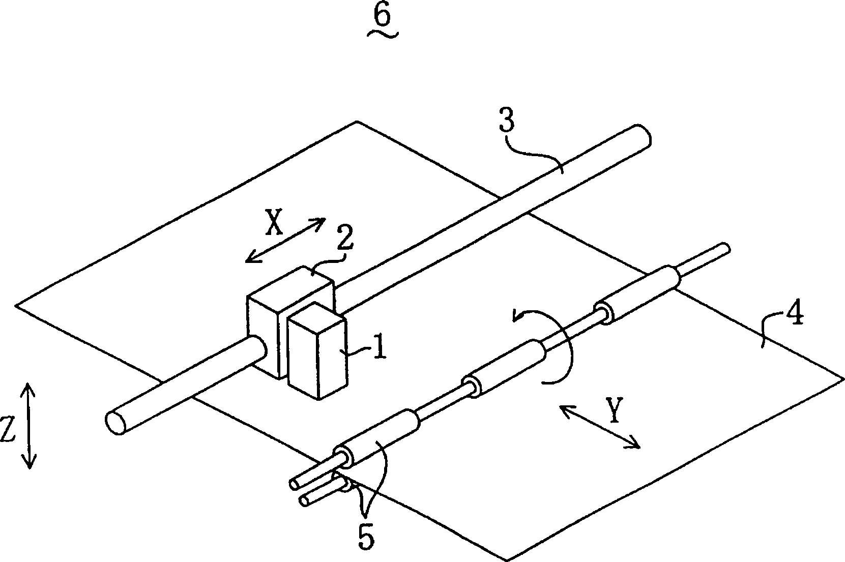
[0126] Such as figure 1 As shown, the inkjet head 1 related to the embodiment is installed in an inkjet printer 6 as an inkjet recording device, and ejected ink hits a recording medium 4 such as paper to perform recording. The inkjet head 1 is mounted on a carriage 2 that reciprocates along a carriage shaft 3 , and reciprocates together with the carriage 2 in the main scanning direction (X direction in the figure). The rollers 5 are configured to convey the recording medium 4 in the sub-scanning direction (Y direction in the figure) every time the carriage 2 scans and moves in the main-scanning direction.
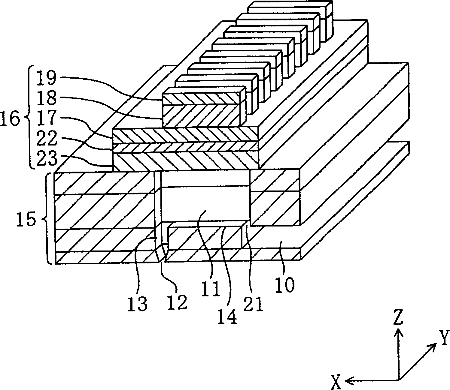
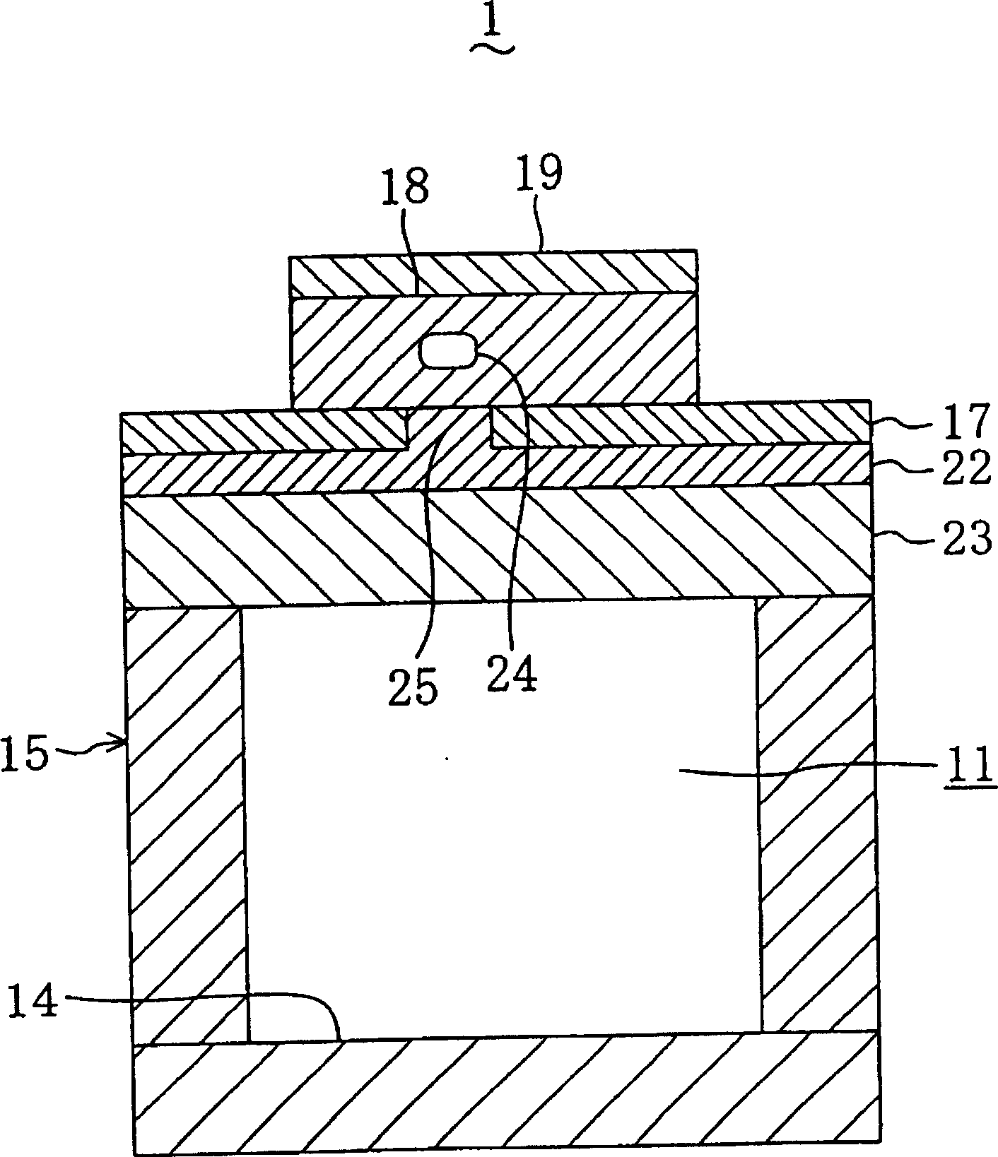
[0127] Such as figure 2 As shown, the inkjet head 1 is provided with an inkjet head main body 15 formed with a common ink chamber 10, a plurality of pressure chamber recesses 14 and a plurality of nozzles 12, and a regulator for transmitting the pressure to the ink in the pressure chamber 11. Section 16.
[0128] The pressure chambe...
Embodiment 2
[0146] Such as Figure 8 As shown, the inkjet head 1a related to the second embodiment is an inkjet head in which the vibrating plate 23 corresponding to each pressure chamber 11 is formed independently. A common electrode 17 made of platinum with a thickness of 0.1 μm to 0.2 μm is provided on the surface side of the inkjet head main body 15 so as to cover the pressure chamber recesses 14 . A piezoelectric body 18 composed of a PZT thin film with a thickness of 3 μm was provided on the surface of the common electrode 17 , and an individual electrode 19 composed of platinum with a thickness of 0.1 μm was provided on the surface of the piezoelectric body 18 . An insulating layer 20 filling a gap between adjacent individual electrodes 19 is formed on the sides and above the individual electrodes 19 to prevent a short circuit between the individual electrodes 19 . Vibration plates 23 made of chromium and having a thickness of 4 μm are formed on the surface of the insulating layer...
Embodiment 3
[0156] It is also not necessary to separately arrange the insulating layer 22 and the vibrating plate 23 as in Embodiment 1 (refer to image 3 ) but as Figure 12 An insulating vibrating plate 23 a serving also as an insulating layer 22 is provided as shown.
[0157] In such an inkjet head, an insulating vibrating plate 23a is formed on the upper electrode 33 instead of forming the insulating layer 22 on the upper electrode 33 in Example 1 (insulating layer forming process) and the vibrating plate 23 is formed on the insulating layer 22. (diaphragm lamination process) obtained.
[0158] Also, if Figure 13 As shown, instead of sequentially forming the insulating layer 20 and the vibration plate 36 on the individual electrode 19 in the second embodiment, the insulating vibration plate 23 a may be formed on the individual electrode 19 .
PUM
 Abstract
Description
Claims
Application Information


