Semiconductor device

a technology of semiconductor devices and semiconductors, applied in semiconductor devices, diodes, electrical apparatus, etc., can solve problems such as device damage, non-uniform current or current oscillation, delay in protection or unstable oscillation,

Active Publication Date: 2016-10-11
FUJI ELECTRIC CO LTD +1
View PDF86 Cites 8 Cited by
  • Summary
  • Abstract
  • Description
  • Claims
  • Application Information

AI Technical Summary

Benefits of technology

[0056]As set forth above, according to the above embodiments, a current detection device is protected from being destroyed under reverse bias. Insulation breakdown at a gate insulator of the current detection device under reverse bias is prevented.

Problems solved by technology

For an IGBT device which controls large amounts of power, there is a problem in that when extremely large current flows, the device is destroyed.
When high voltage is applied or large current flows, gate voltage becomes unstable causing non-uniform current or current oscillation.
For an IGBT having a current detection function, there is a problem in that delay of protection or unstable oscillation is likely to occur because a feedback loop starting from detection of large current up to reduction of the gate voltage is long.

Method used


Image

  • Semiconductor device
  • Semiconductor device
  • Semiconductor device

Examples


tenth embodiment

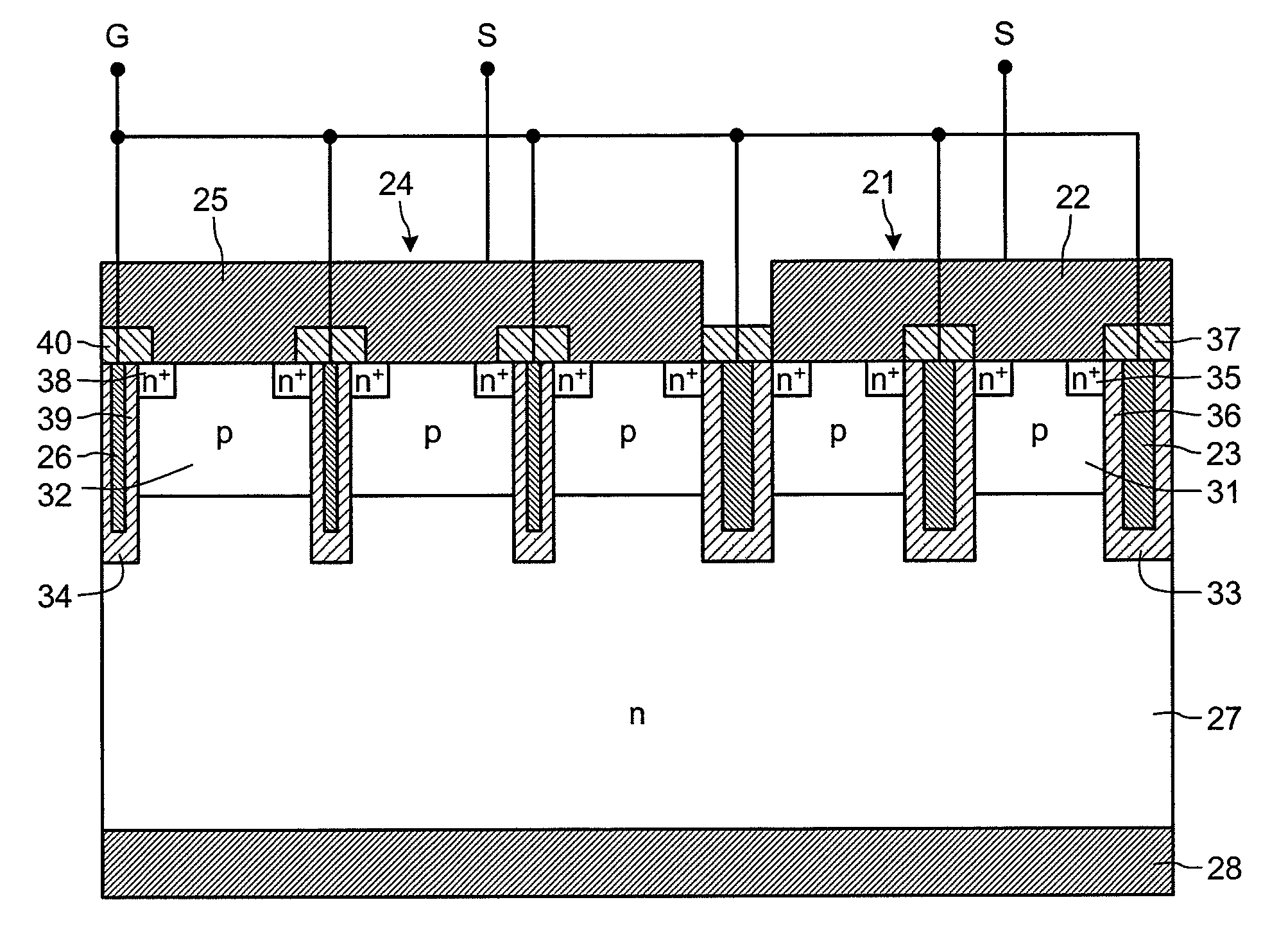
[0129]FIG. 10 is a plan view illustrating a configuration of a semiconductor device having a current detection function according to a tenth embodiment. FIG. 11 is a cross-sectional view of the semiconductor device having a current detection function according to the tenth embodiment. As depicted in FIG. 11, the semiconductor device having the current detection function includes a main device 24 and a current detection device 21 separated from the main device 24. The current detection device 21 is formed in a current detecting structure region of the same substrate as the main device 24. Therefore, the current detection device 21 and the main device 24 share an n-drift layer 27, a p-collector layer 42, and a collector electrode 28.

[0130]In FIG. 11, the main device 24 and the current detection device 21 are about the same size. However, actually, the surface area of the current detection device 21 is several tenths smaller than that of the main device 24. Therefore, reflecting the ra...

eleventh embodiment

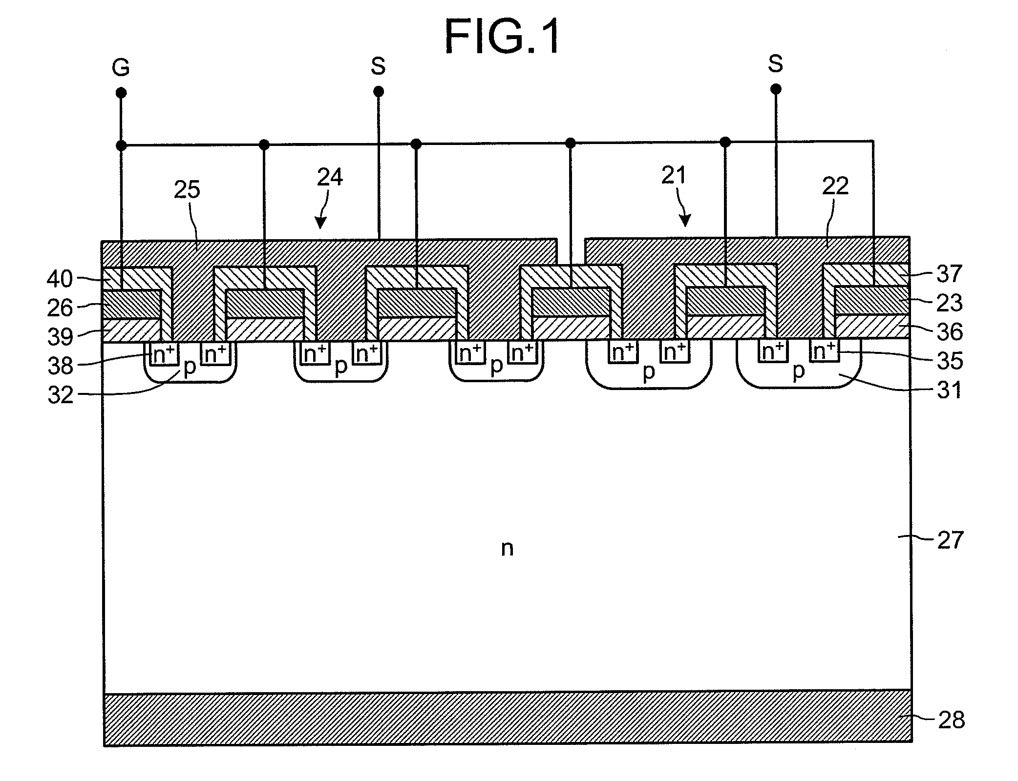
[0136]FIG. 12 is a cross-sectional view of a semiconductor device having a current detection function according to an eleventh embodiment. As depicted in FIG. 12, according to the eleventh embodiment, the current detection device 21 has a third dummy trench IGBT structure 103 compared with the tenth embodiment. In the current detection device 21, the dummy trench electrodes 85 are not connected to the trench gate electrodes 83 and 84 but are connected to the p-type floating layer 81 in a region that is not depicted in the drawing. As a result, potential of the current detection device 21 becomes stable. The p-type floating layer 81 is also connected to the emitter electrode. Accordingly, potential of the p-type floating layer 81 becomes identical to potential of the emitter electrode 22, the p-type floating layer 81 not being electrically isolated from the emitter electrode 22. In this way, the withstand voltage of the current detection device 21 becomes higher than the main device ...

twelfth embodiment

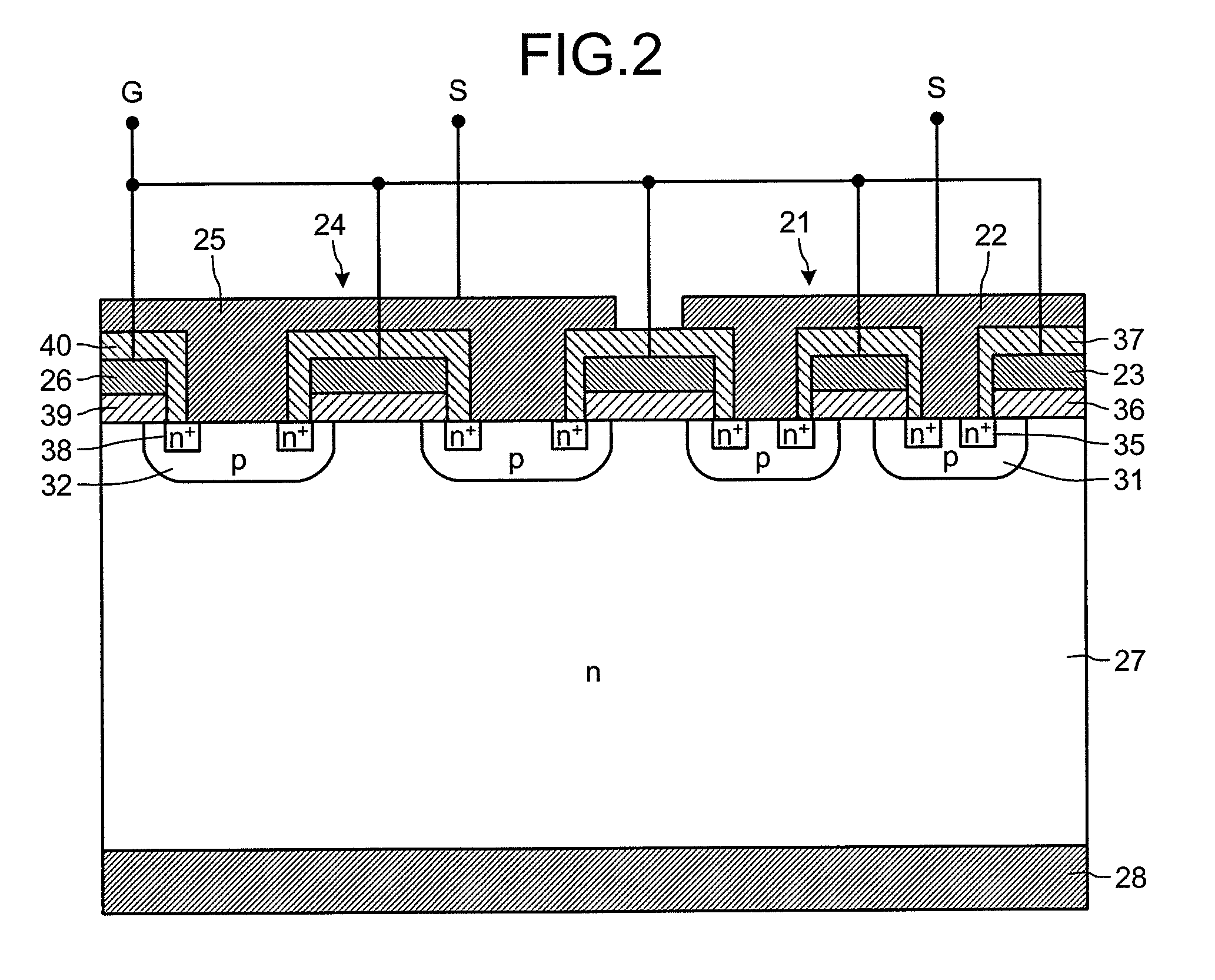
[0137]FIG. 13 is a cross-sectional view illustrating a semiconductor device having a current detection function according to a twelfth embodiment. In the twelfth embodiment, the current detection device 21 has a fourth dummy trench IGBT structure 104 compared with the tenth embodiment and the eleventh embodiment. In the current detection device 21, the dummy trench electrodes 85 are electrically connected to the emitter electrode 22. Therefore, the dummy trench electrodes 85 and the emitter electrode 22 have identical potential and thus, potential of the current detection device 21 becomes stable. The p-type floating layers 81 are separated from the emitter electrode 22 by the interlayer insulator 37. Thus, the p-type floating layers 81 are electrically isolated (floating) from the emitter electrode 22. In this way, the withstand voltage of the current detection device 21 becomes higher than the main device 24.


PUM


Abstract

Between a source electrode (25) of a main device (24) and a current sensing electrode (22) of a current detection device (21), a resistor for detecting current is connected. Dielectric withstand voltage of gate insulator (36) is larger than a product of the resistor and maximal current flowing through the current detection device (21) with reverse bias. A diffusion length of a p-body region (32) of the main device (24) is shorter than that of a p-body (31) of the current detection device (21). A curvature radius at an end portion of the p-body region (32) of the main device (24) is smaller than that of the p-body (31) of the current detection device (21). As a result, at the inverse bias, electric field at the end portion of the p-body region (32) of the main device (24) becomes stronger than that of the p-body region (31) of the current detection device (21). Consequently, avalanche breakdown tends to occur earlier in the main device 24 than the current detection device (21).

Description

TECHNICAL FIELD[0001]The present invention relates to a semiconductor device that detects current.BACKGROUND ART[0002]Among insulated gate semiconductor devices such as metal-oxide-semiconductor field-effect transistors (MOSFET) and insulated gate bipolar transistors (IGBT), a technology has been disclosed where one semiconductor chip includes a main insulated gate semiconductor device (hereinafter, main device) and a small-size insulated gate semiconductor device for current detection (hereinafter, current detection device) that is separate from the main device and shares a gate and drain terminal with the main device (see, for example, Patent Documents 1, 2, and 3 below). A resistor for current detection is connected with a source terminal of the current detection device so that very small electrical current proportional to the current flowing through the main device is detected by a voltage drop at the resistor. According to the insulated gate semiconductor devices having such a ...

Claims


Application Information

Patent Timeline
Patent Type & Authority Patents(United States)
IPC IPC(8): H01L29/78H01L29/96H01L29/739H01L29/08H01L29/10H01L29/423
CPCH01L29/7815H01L29/7395H01L29/7397H01L29/0878H01L29/1095H01L29/4236H01L29/7813H01L27/0629H01L27/0658H01L29/0696H01L29/7827
Inventor MOMOTA, SEIJIABE, HITOSHISHIIGI, TAKASHIFUJII, TAKESHIYOSHIKAWA, KOHIMAGAWA, TETSUTAROKOYAMA, MASAKIASAI, MAKOTO
Owner FUJI ELECTRIC CO LTD
Why Eureka
Try Eureka