

Cleaning method for substrate processing chamber, storage medium, and substrate processing chamber
A substrate processing and cleaning method technology, applied in cleaning methods and appliances, chemical instruments and methods, discharge tubes, etc., can solve the problems of oxide film insulation damage, stability, difficult plasma state, etc., and achieve the effect of inhibiting the reaction
- Summary
- Abstract
- Description
- Claims
- Application Information
AI Technical Summary
Problems solved by technology
Method used
Image

Examples
Embodiment Construction
[0041] Hereinafter, embodiments of the present invention will be described with reference to the accompanying drawings.
[0042] First, a plasma processing apparatus applied to the cleaning method of the substrate processing chamber in each embodiment of the present invention described later will be described.
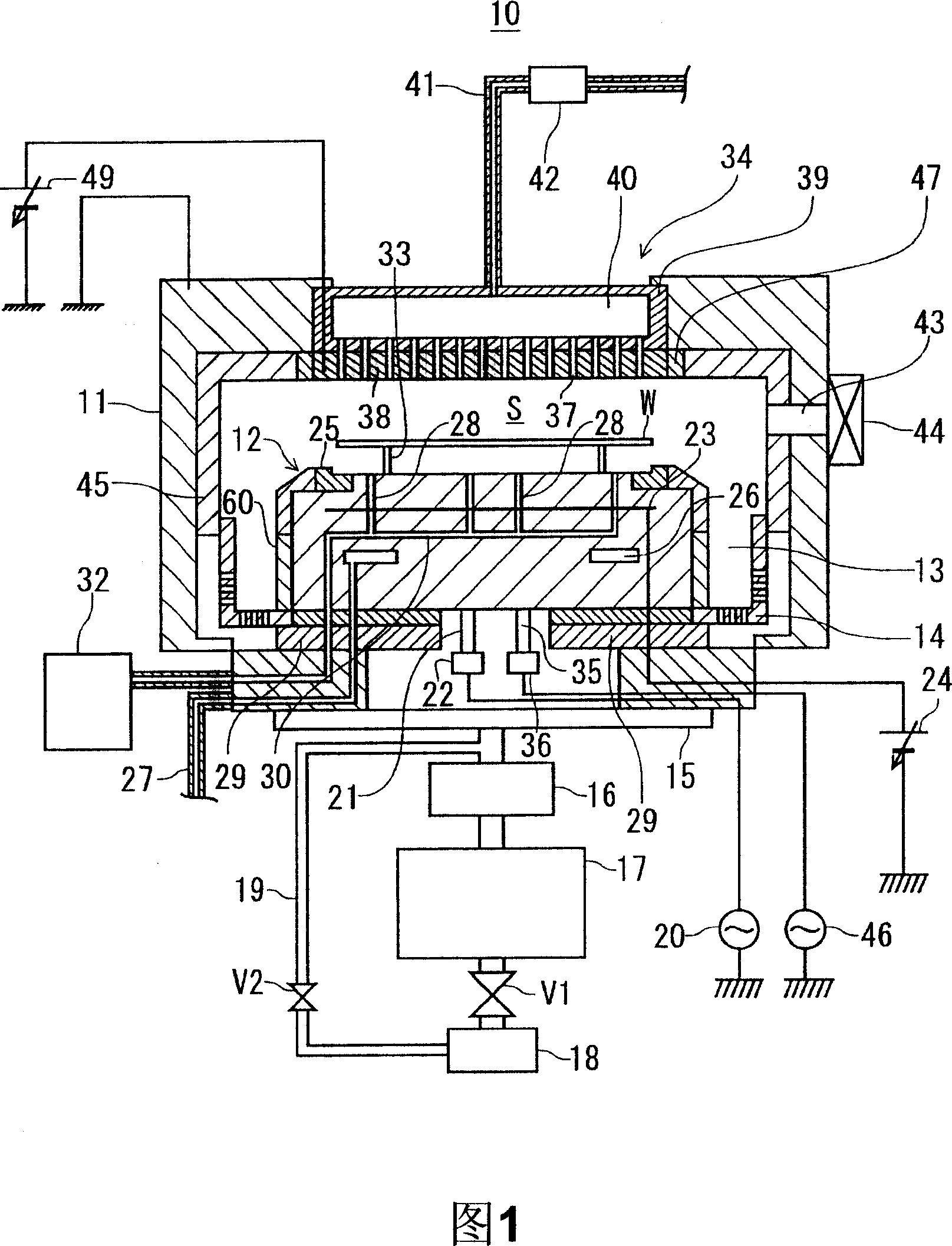
[0043] 1 is a cross-sectional view showing a schematic configuration of a plasma processing apparatus applied to a cleaning method of a substrate processing chamber in each embodiment of the present invention. This plasma processing apparatus is configured to be capable of performing RIE (Reactive Ion Etching) processing or ashing processing on a semiconductor wafer W serving as a substrate.
[0044] In FIG. 1 , the plasma processing apparatus 10 has a cylindrical substrate processing chamber 11 having a processing space S therein. In addition, in the substrate processing chamber 11, for example, a cylindrical susceptor 12 having a diameter of 300 mm is arranged as a ...
PUM
 Abstract
Description
Claims
Application Information