
Electrooptic device, method for manufacturing same, and electronic apparatus

An electro-optic device and electro-optic technology, applied in the direction of electric light sources, identification devices, lighting devices, etc., can solve the problems of being unable to install other components, the appearance of electro-optic devices becoming larger, and the difficulty of miniaturization of electro-optic devices

Active Publication Date: 2005-02-02
BOE TECH GRP CO LTD
View PDF1 Cites 6 Cited by
  • Summary
  • Abstract
  • Description
  • Claims
  • Application Information

AI Technical Summary

Problems solved by technology

Therefore, it is difficult to miniaturize the electro-optic device as a whole because it increases the size of the electro-optic device.
Furthermore, since the control circuit board is only electrically connected to the driver IC, there is a problem that other components other than the electronic components constituting the drive circuit unit cannot be mounted.

Method used


Image

  • Electrooptic device, method for manufacturing same, and electronic apparatus
  • Electrooptic device, method for manufacturing same, and electronic apparatus
  • Electrooptic device, method for manufacturing same, and electronic apparatus

Examples


no. 1 approach

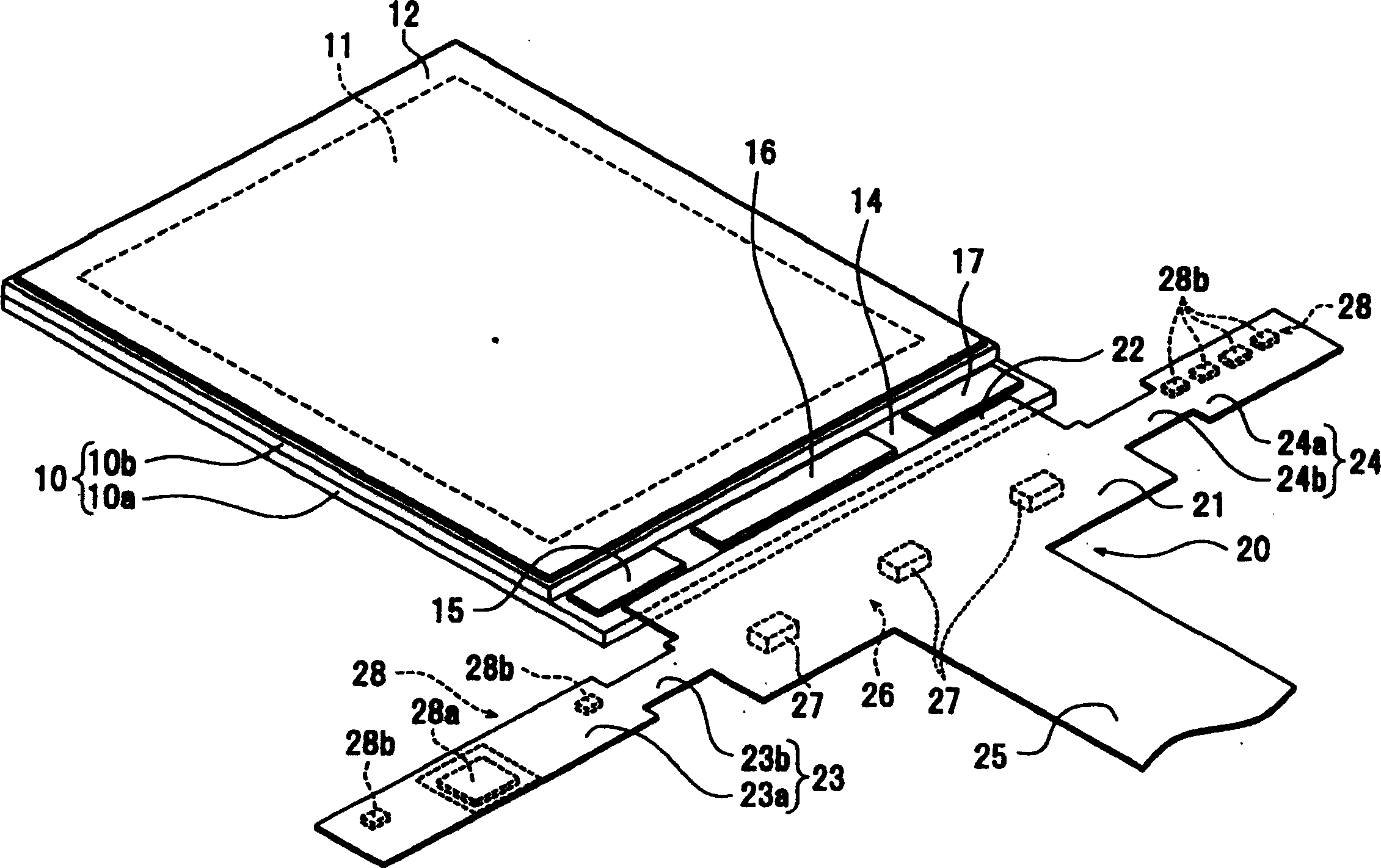
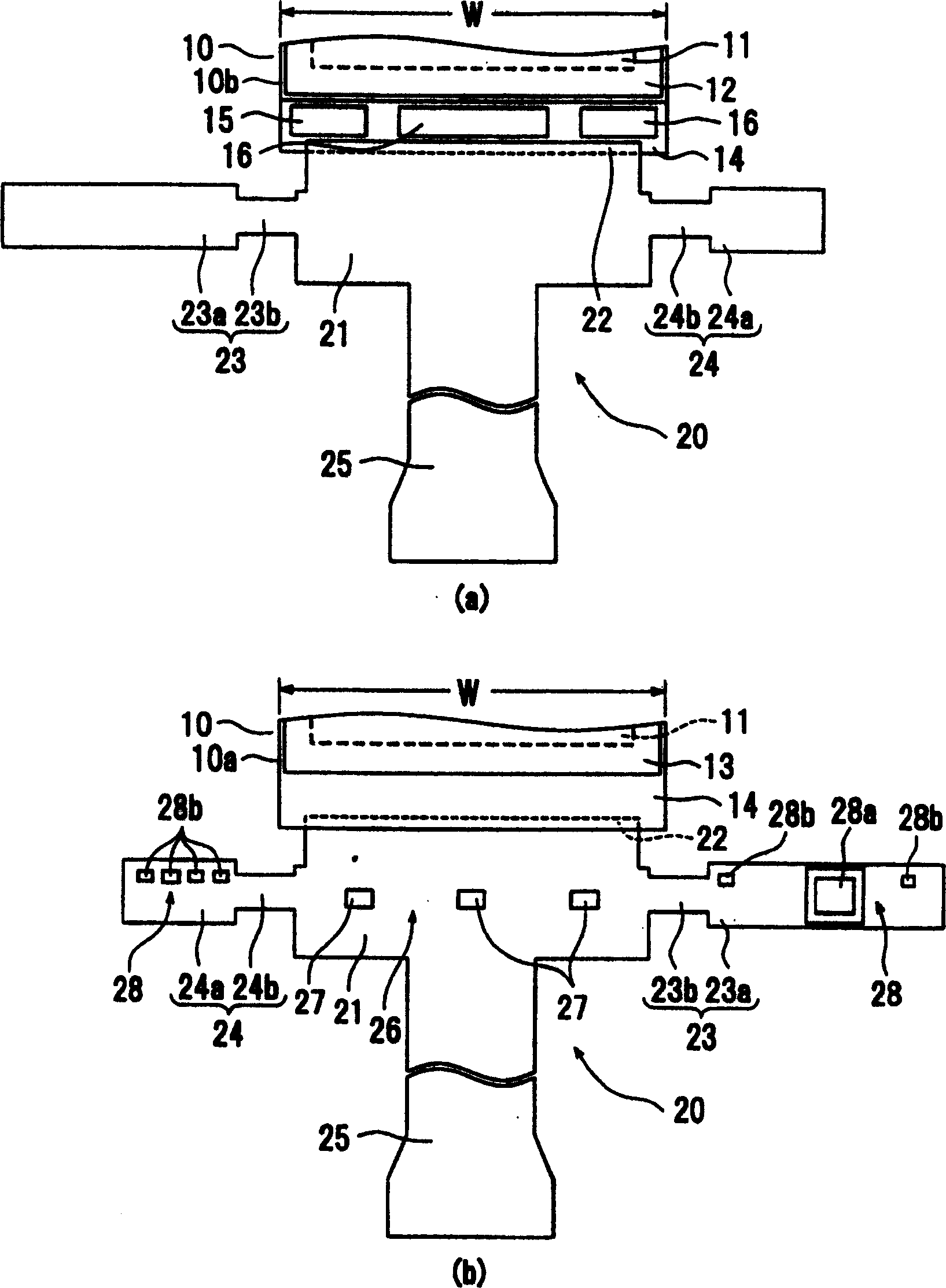
[0049] figure 1 as well as figure 2 It is a figure which shows the example of the structure of an electro-optical panel and an interface substrate. Such as figure 1 as well as figure 2 The electro-optical panel 10 and the interface substrate 20 shown are components mounted on electronic equipment such as mobile phones. The electro-optical panel 10 is a hard substrate such as a glass substrate, and is provided with an image display unit 11 . The image display unit 11 is composed of a plurality of pixels. Here, the electro-optic device is, for example, a liquid crystal display device formed by encapsulating liquid crystal with a sealing material between two substrates of the first electro-optic panel 10 a and the second electro-optic panel 10 b of the electro-optic panel 10 . In addition, above and below the image display unit 11, polarizing plates 12 and 13 for polarizing light from LED 27 serving as a light source unit 26 to be described later are provided.

[0050] Fu...

no. 2 approach

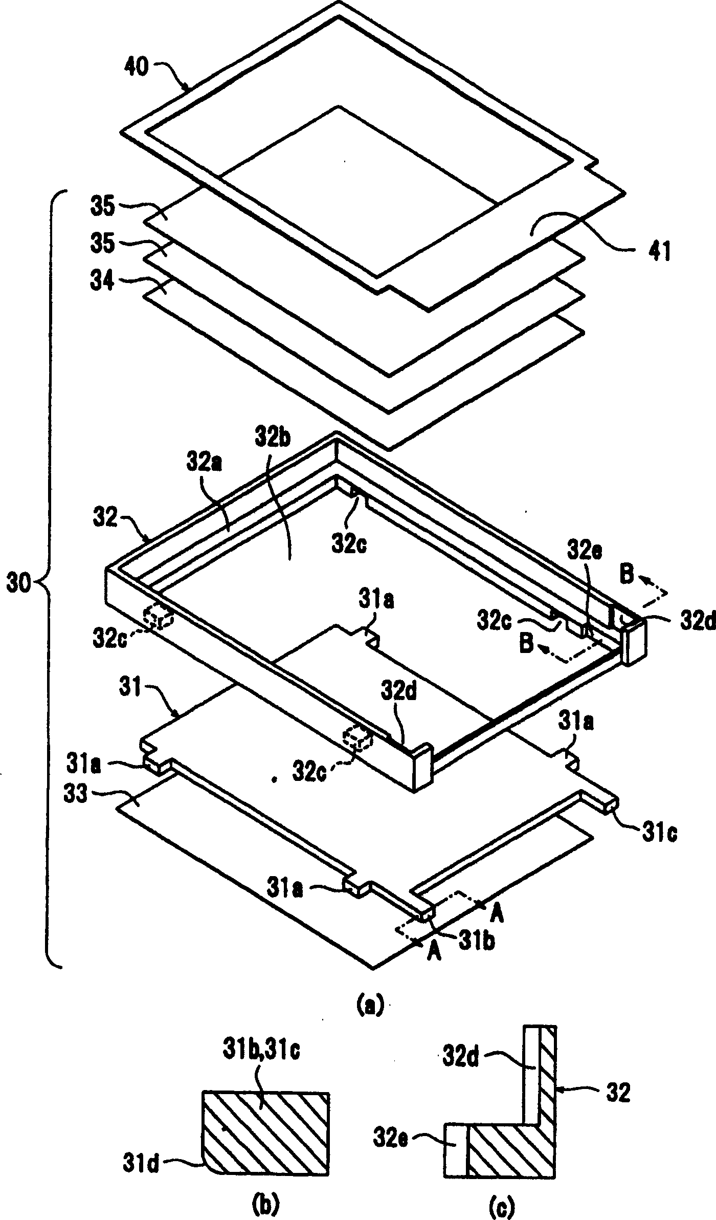
[0071] Figure 11 It is a figure which shows another structural example of the case of this invention. Figure 12 is a diagram showing a structural example of the electro-optical device according to the second embodiment. Figure 12 The electro-optic device 1' shown with Figure 9 The electro-optic device 1 shown in (b) is different in that the protrusions 23, 24 are bent toward the surface of the electro-optic panel 10 through the notch 32f provided on the outer peripheral surface of the housing 32'. In addition, due to the removal of the electro-optical panel 10, the interface substrate 20, and the housing 32 of the light guide unit 30, part of the basic structure is different from the Figure 9 The electro-optical device 1 shown in (b) is substantially the same, and therefore its description is omitted. Here, the electro-optical device 1' and Figure 9 The electro-optic device 1 shown in (b) also has a COG structure.

[0072] Such as Figure 11 As shown, the case 32' ...


PUM


Abstract

An electrooptic device is provided that comprises an electrooptic panel having an image display region for displaying an image and an interface substrate connected to the electrooptic panel via a connection part. The interface substrate has a folding part folded at the connection part toward a lower-surface side of the electrooptic panel and projections extending from the folding part positioned at the lower-surface side of the electrooptic panel. The projections are folded toward a top-surface side of the electrooptic panel so that electronic parts of the projections are opposed to driver ICs that are mounted on an overhanging part of the electrooptic panel.

Description

technical field [0001] The present invention relates to an electro-optical device, a manufacturing method, and an electronic device, and more particularly, to an electro-optical device, a manufacturing method, and an electronic device in which electronic components mounted on an interface substrate are arranged to face the front or back of an electro-optic panel. Background technique [0002] An electro-optical device such as a liquid crystal display device is generally an electro-optic panel having an image display section composed of a plurality of pixels composed of liquid crystals, etc., and a drive circuit composed of a plurality of electronic components required to drive the image display section. An interface substrate for connecting the electro-optical panel to electronic equipment such as a mobile phone, a light source for irradiating light to the light guide plate, and a light guide plate for emitting light irradiated from the light source to the image display unit....

Claims


Application Information

Patent Timeline
Patent Type & Authority Applications(China)
IPC IPC(8): G02F1/1333G02F1/13G02F1/1345G09F9/00H01L51/50H05B33/06H05B33/14
CPCH05K2201/052H05K2201/056G02F1/13452H05K2201/10136H05K1/189G02F1/1345
Inventor 平野善久
Owner BOE TECH GRP CO LTD
Learn More