Organic luminous display apparatus and manufacturing method thereof

A light-emitting display, organic technology, applied in the field of organic light-emitting display devices, can solve problems such as affecting the quality of the display

Active Publication Date: 2005-03-16
AU OPTRONICS CORP
View PDF0 Cites 1 Cited by
  • Summary
  • Abstract
  • Description
  • Claims
  • Application Information

AI Technical Summary

Problems solved by technology

Cathode with high impedance value leads to serious voltage drop problem, which greatly affects the quality of the display

Method used


Image

  • Organic luminous display apparatus and manufacturing method thereof
  • Organic luminous display apparatus and manufacturing method thereof
  • Organic luminous display apparatus and manufacturing method thereof

Examples


Embodiment 1

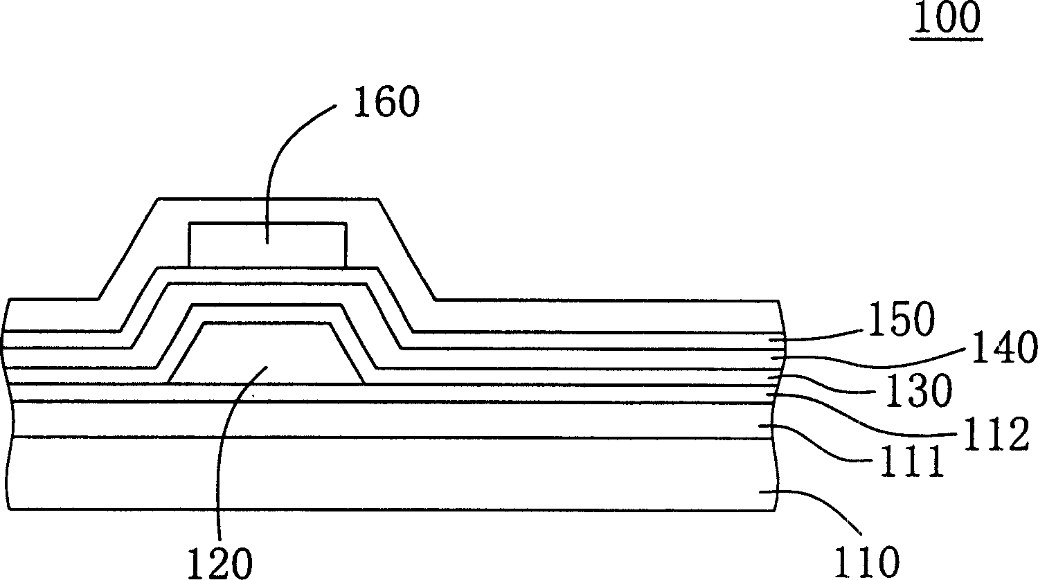
[0017] Please refer to figure 2 , which shows a side view of an organic light emitting display unit according to Embodiment 1 of the present invention. In the organic light emitting display unit 100, a reflective layer 111 is formed on the substrate 110, the thin film transistor 120 is disposed on the reflective layer 111; the anode 130 is disposed on the thin film transistor 120 and the substrate 110; the organic light emitting structure 140 is disposed on the anode 130; 150 is disposed on the organic light emitting structure 140 ; ​​the bus line 160 is formed on the cathode 150 and is electrically connected to the cathode 150 to reduce the resistance of the cathode 150 .

[0018] In the organic light-emitting display unit 100, the cathode 150 is made of a light-transmitting material, such as a layer of thin-film metal, a layer of indium tin oxide (ITO) or a layer of thin-film metal and at least one layer of indium. A combination of tin oxides. In addition, the thickness o...

Embodiment 2

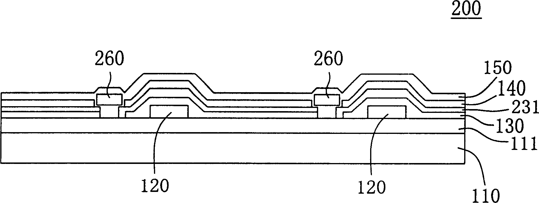
[0023] The components of the organic light emitting display unit of this embodiment are the same as those of the first embodiment, but the relative positions of formation are different, and the manufacturing process is also different. This embodiment will continue to use the component numbers of the first embodiment.

[0024] Please refer to image 3 , which shows a side view of an organic light emitting display unit according to Embodiment 2 of the present invention. In the organic light emitting display unit 200 , a protective layer 231 is disposed between the anode 140 and the bus line 260 , so that the anode 140 is adjacent to the bus line 260 but is not electrically connected. In addition, the bus line 260 is disposed on the sides of the organic light emitting structure 140 and the cathode 150 , and is located between two organic light emitting units to form a black matrix.

[0025] In an actual manufacturing process, the manufacturing method of the organic light emitti...


PUM


Abstract

The invention is an organic light-emitting display, namely OLED which including a base board and several organic light-emitting display units. The organic light-emitting display unit includes: film transistor, positive electrode, organic light-emitting structure, negative electrode and bus line. The film transistor is arranged on the base board. The positive electrode is arranged on the film transistor and the base board. The organic light-emitting structure is arranged on the positive electrode. The negative electrode is arranged on the organic light-emitting structure, the bus line is connected to the negative electrode electrically in order to reduce the resistance of the negative electrode.

Description

【Technical field】 [0001] The present invention relates to a display device, and in particular to an organic light emitting display device. 【Background technique】 [0002] In recent years, an organic light-emitting display (OLED) has gradually attracted attention in the display market due to its simple structure, excellent operating temperature and response speed, sharp color contrast, and no viewing angle limitation. [0003] Please refer to figure 1 , which is shown in accordance with the schematic diagram of a conventional bottom-emission organic light-emitting display device. A bottom emission organic light emitting display device 10 includes a substrate 11 , a thin film transistor 12 , a protective layer 13 , an anode 15 , an organic light emitting layer 16 , a cathode 17 and a spacer 18 . The anode 15 is a transparent indium tin oxide electrode, and the substrate 11 is also a transparent glass substrate. In the bottom emission organic light emitting display device 10...

Claims


Application Information

Patent Timeline
Patent Type & Authority Applications(China)
IPC IPC(8): H05B33/10H05B33/12H05B33/20H05B33/22H05B33/26
Inventor 苏志鸿
Owner AU OPTRONICS CORP
Why Eureka
Try Eureka